This thread has been locked.

If you have a related question, please click the "Ask a related question" button in the top right corner. The newly created question will be automatically linked to this question.

Pulseox TIA Circuit Line Noise

Other Parts Discussed in Thread: AFE4400, OPA333, TINA-TI, OPA381

We are having a problem with line noise with our pulse oximeter circuit, which is based on a TI reference design. We want to modify the circuit to eliminate this sensitivity and we are seeking advice on the circuit shown here:

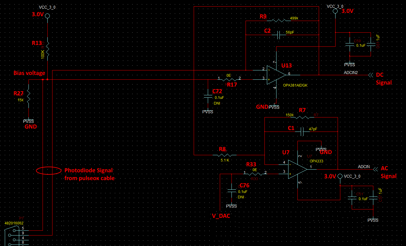
We had noted a line noise problem in our prototype and thought it would be improved in the layout for our final board. We were advised by a TI engineer to add pads for C72 and R17 on non-inverting input of stage 1 and pads for C76 and R33 on non-inverting input of stage 2. This was done so that we could fix the noise problem if it persisted. Well, it did persist and I don't have the name of the original engineer that made this suggestion so I am posting here for advice.

An optimal solution for us would be populating C72 and/or changing the zero ohm jumper at R17, but I am guessing we may have to decrease the bandwidth of the TIA by changing C2 and or R9 (not optimal as component removal step is involved). I suppose there could even be a problem with the biasing of provided by the R13/R27 voltage divider of about 0.39V.

We were also working on modeling this circuit on LTSpice, but it appears it would be wiser to go with TINA as we would have access to the OP333 and OP381 models. If we must do a simulation then we would also need advice on simulating the photodiode (we have the spec sheet from the mfg of the cable, but no model for the photodiode itself).

Thanks in advance for your help and kind advice,

Kevin

PS: The new product is using the AFE4400, which was still in beta when this design was done

  • Hi Kevin,

    Line noise pickup and amplification problems can be difficult to solve because of the strong line voltage fields inside most indoor buildings, and because of the very high transimpedance gain associated with most photodiode amplifiers. Man-made light could modulate the photodiode current at the line frequency if the photodiode is exposed to it. Or, the line voltage's field could be coupling into the photodiode cable, or circuit board, which is then being amplified by the op amp circuit.

    Often line noise is picked up as a common-mode signal riding on both the input line and ground. But because the op amp configurations don't provide a matched gain through each input path the common-mode noise is converted to differential noise and is amplified.

    I do have some questions:

    • Is the line noise being observed at the DC signal, AC signal, or both outputs?
    • Is the line noise observed at the output when the photodiode and cable are disconnected from the amplifier board?
    • What kind of enclosure does the circuit get packaged in?

    You mention a TI pulse oximeter reference design. By chance is this what you were referencing?

    There are ways to employ differential transimpedance amplifiers that take advantage of an op amp's common-mode rejection to reduce noise response. The circuits are more complex than what you are currently using.

    If your simulation software doesn't include a model for your photodiode, check the company's product web pages or contact their applications department for help.  

    Regards, Thomas

    PA - Linear Applications Engineering

  • Hi Thomas,

    Thanks for the fast response! The book link you provided is not the source of the design (Thanks...much appreciated link). It was these application notes:

    http://www.ti.com/lit/an/sprab37a/sprab37a.pdf

     http://www.ti.com/lit/an/slaa274b/slaa274b.pdf

    and http://www.ti.com/lit/an/slaa458/slaa458.pdf

    Here is what we know from some rudimentary experiments:

    1. It is not due to ambient light
    2. When we became aware of the problem we were able to recreate in-house by shifting the board near to a noise source (a laptop power cord)
    3. When the noise problem is occurring if the person with the pulesox on touches  the USB connector shell on the board and the problem is reduced/eliminated.
    4. The amplitude of the noise is typically no more than the amplitude of the AC pulse ox waveform (usually about 30%). It's typical 50Hz hash.
    5. We get less noise using a pulseox cable that has different properties for the photodiode's wires (including the configuration of the shielding in the cable),

    In answer to your questions:

    • Is the line noise being observed at the DC signal, AC signal, or both outputs?  The noise is on the first stage DC output (and hence also on the AC output). I don't have a scope sensitive enough to view the waveform that is input to the first stage. My working assumption is the noise is coupled into the photodiode signal on our board prior to the first stage amp circuitry because of the variation we see in the pulseox cable.
    • Is the line noise observed at the output when the photodiode and cable are disconnected from the amplifier board? Very good question. I did not check for this. I'm assuming not, but I will check and update the post
    • What kind of enclosure does the circuit get packaged in? It is ABS plastic only; although we are adding a shield over a portion of the PCB to eliminate some radiated USB clock noise for EN 60601-1-2 compliance.

    You might be able to advise us in this regard: we are planning on shifting to TINA-TI in order to use the OPA333/381 models. We are currently using LTSpice. Furthermore, the photodiode is part of an assembly that includes the IR/Red LEDs so it looks like we will model it as a current source with Ci. 

    Because we can get more or less AC noise depending on the pulseox cable type we were assuming that the problem could be fixed by going to a pulseox cable with more substantial shielding in the photodiode lines (even though the current cable works fine for Nonin). This only helped marginally but seems to suggest that the fix would be trying to remove the AC at/inside of the first stage. Since I just had a look at the application notes once again it seems like we may want to change the R and/or C in the first stage feedback path. I have an engineer working on simulating the same as well as adding some R and C to the non-inverting input to the first stage.

    As I mentioned, we are shifting to the AFE4400 for the next version of the PCB, so we are expecting to eliminate the problem going forward. However, this is still an important problem to solve w.r.t. current stock.Please give us your directions. We don't have all the resources we need to do a thorough analysis/design, but we believe we can cut and try based on your experiences. 

    Kind regards,

    Kevin

  • Hi Kevin,

    It sounds like you are on the right path using the more complete shielded cable and adding shielding internal to the enclosure. Your results thus far tend to support the idea that the 50 Hz noise is common-mode noise. Unfortunately, 50 Hz is a low frequency and shielding needs to be thick for high attenuation. However, thin shielding is definitely better than no shielding.

    The natural engineering tendency is to try and filter out offending noise. But if the noise is common-mode in nature, then the filter has to be a low-frequency common-mode filter to be effective. Practical common-mode filters topologies accomodate balanced, differential inputs that are associated with difference amplifiers and instrumentation amplifiers. Your Pulseox circuit uses a single-ended input OPA381 TIA, and OPA333 voltage-feedack stage and those are not balanced input designs. Then there is the issue of the bandwidth required for the actual Pulseox signal. If 50 Hz is within the required Pulseox bandwidth you don't want a filter eliminating that frequency.

    Since you are planning to go with a newer design that uses the AFE4400, see if you can get the 50 Hz level to an acceptable level with the previously mentioned shielding.

    Regards, Thomas

    PA - Linear Applications Engineering