This thread has been locked.

If you have a related question, please click the "Ask a related question" button in the top right corner. The newly created question will be automatically linked to this question.

Input 4/20mA / 0/10V

Other Parts Discussed in Thread: INA188, TINA-TI, TIPD195, INA333

Hi everybody,

I'm looking for a solution of my problem, but I cannot find any answers by myself so I'm requesting your help.

For our new product, we'll develop an analog input module (as we can find with PLC...). Our module will be able to do 0/10V and 4/20mA. For the moment, I have three terminals for each input (One for Voltage input +, one for current input +, and for input - ). My problem is that I would to do the conversion of 0/10V o 4/20mA to 3V3 without any selection switch (especially to include or not the shunt resistor used to convert 4/20mA).

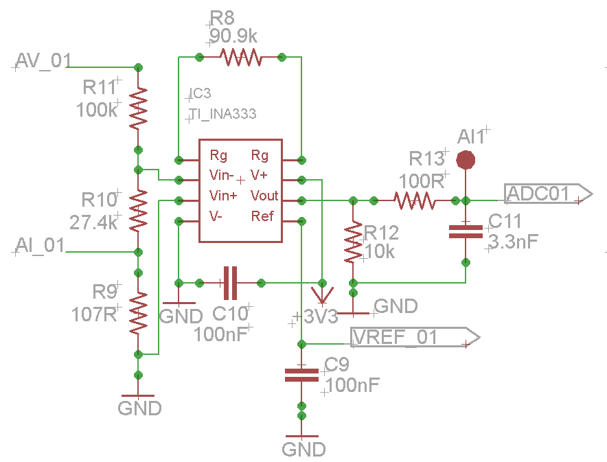
You'll find my diagram in enclosed documents. If you have any suggestion to improve it, I'll be very happy.

Thank you in advance,

Best regards,

Fabrice

DIAGRAM.pdf

  • Hello Fabrice,

    We've worked on other designs similar to this one and the overall design method is valid.  Consider putting your design into TINA-TI SPICE to test the behavior and adjust the gain / scaling if required.  Also, we created a similar design that you may find interesting:  TIPD195 - 3-Terminal PLC Input reference design.   

  • Hi Collin,

    Thank you for your diagram. I'll look it, and ask you if I have some questions.

    Best regards,

    Fabrice

  • Hi Collin,

    I just look your design, it's very interesting but I think some points will be very difficult for us.

    On my module, there will be 8 channels, INA188 has only one channel, so I will need 8 INA188, but is there another reference which can has more channels (2 or 4) ?

    Moreover, in this design, INA188 is supplied with + or - 15V, is it compulsory to do that, because the output voltage is between 0.2 and 4.8V, so is it possible to supply it between 0 and 3V3 ? Then, my µc accepts voltage up to 3V3, so I think I need to recalculate resistors to adap the output voltage and also the power supply.

    For example, I can put Vref at 1.66V and output voltage can be between 0.2 and 3.1V, do you think it's possible ? Because I'm trying to simulate it with TINA-TI, but 1,66V is for 0V and not for 5V. So, it means that my input will be between 0 and 10V.

    Thank you in advance,

    Best regards,

    Fabrice Péden
  • Hello Fabrice,

    The INA188 will not work with a +3.3V supply.  Consider using the INA333.  You can modify the TINA files associated with TIPD195 to use the INA333 and the different voltage scaling ratios that you determined using the equations from the design guide.

  • Hello Collin,

    Thank you for this information.

    I'm trying to do that. To simulate the INA333, I have just to modify the value of resistor of INA188 (150k instead of 20k and 50k instead of 25k) ? Or I need to modify another thing ?

    Thank you in advance,

    Regards,

    Fabrice Péden
  • Attach your simulation file and we'll take a look. Depending on your configuration the input common-mode voltage vs. output voltage may limit the output voltage swing when operating on a 0/+3.3V supply. We'll take a look once we see the circuit.
  • Hello Collin,

    Thank you for your help, I'm also discovering TINA-TI software ;-)

    I have found INA333 in the library, but can I use the same formula than in the TIPD195 document ?

    Regards,

    Fabrice Péden

    TIPD195_functional_with_INA333.TSC

  • Hello Collin,

    I'have try to recalculate values of resistors.

    R1 = 100k

    R2 = ((R1*Vd)/(Vin-Vd)) = ((100k * 400mV)/(10 - 400mV)) = 4.167k

    G = ((Vout - Vref)/(Vd)) = (3.1 - 1.67)/(400mV)) = 3.575

    GINA333 = 100k/(3.575-1) = 39k

    But with these values, I haven't the wished curbe. For me, I'd like to have : Input : 0V --> 0.24V & 10V --> 3.1V

    Regards,

    Fabrice

    8664.TIPD195_functional_with_INA333.TSC

  • Hello,

    Looks like you're getting closer.  Could you share an image of the circuit results you're getting as well as the desired results?  It was a little unclear in your last message. 

    For example: 

    Input = 0-10V

    Output = ?

    Input = 0-20mA

    Output = ?

  • Hello Collin,

    Sorry for my unclear message. Please, find below :

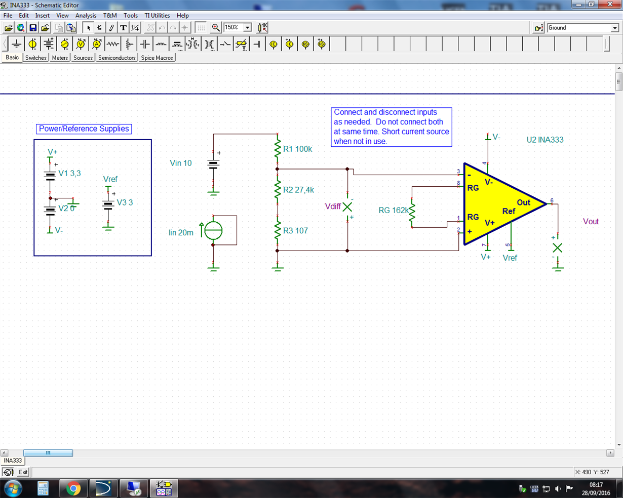
    - My design

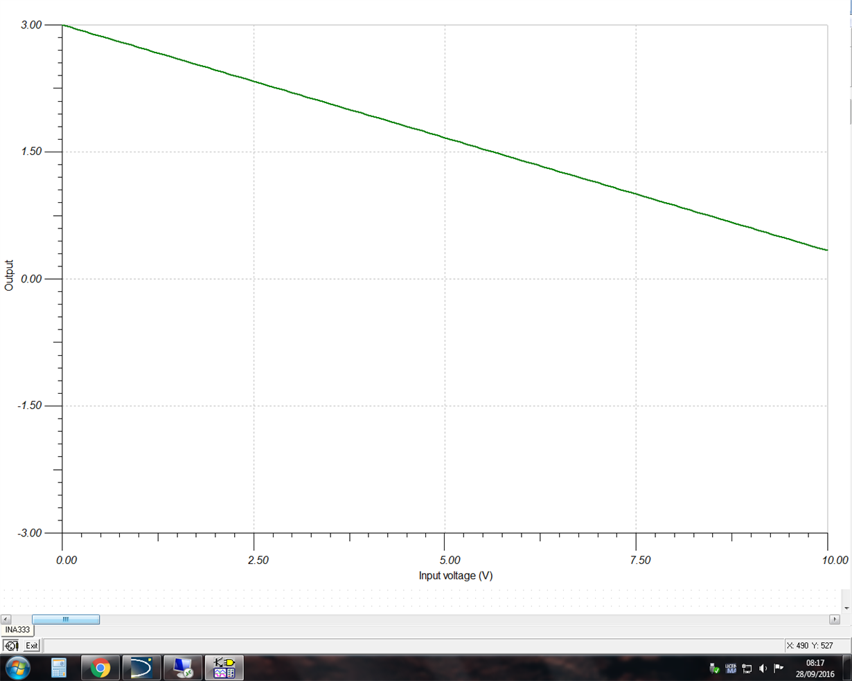
    - result for 0/10v

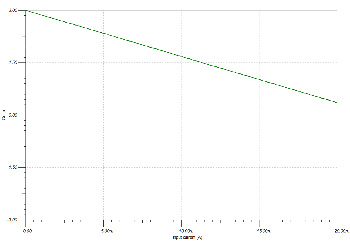
    - result for 4/20mA

    Regards,

    Fabrice Péden

  • Hello Collin,

    Have you take a loot at my design ? What do you think about it ?

    Thank you in advance,

    Regards,

    Fabrice Péden

  • Hi Fabrice,

    I looked over the circuit and it looks to be performing as desired.  Were there any changes or modifications you need to make to the circuit operation?  The 0-10V and 0-20mA signals produce an output voltage of roughly 3V to 60-80mV. 

  • Hello Collin,

    Thank you very much for your help.

    Regards,

    Fabrice Péden

  • Hi Collin,

    I have mounted this diagram in real.

    Voltages seems to be good everywhere (Vin, Vdiff, Vref) according to the waveforms except for Vout. I must have an outpu voltage which comes from 3V to 0.2V. When I measured, for 0V in input, I have effectively 3V, but for 10V in output, I have 3.4V (I think the AOP is in saturation).

    I don't understand what I have these values. It's like my "+" and "-" were inverted, but I've checked everything is good. I tried to make this design two times, on both cards, it's the same.

    If you can help me.

    Thank you,

    Regards,

    Fabrice Péden

  • Hi Fabrice,

    It does sound like the "+" and "-" inputs may be switched. If you input 0.5V, what is the output voltage? If it is greater than 3V (approximately 3.14V) then I believe the "+" and "-" inputs of the INA333 have been switched.

    If inputting 0.5V does not increase the output voltage above 3V, please provide us with a table of measurement results of the output voltage for an input voltage of 0.5, 1V, 1.5V, 2V, etc.

    -Tim Claycomb

  • Hi Tim,

    I have swichted the both inputs. Now, it's working perfectly. But, it's not in agreement with the design, so I don't understand everything. I'll check once again to be sure that I did the good design.

    Thanks

    Regards,

    Fabrice

  • Hi Tim,

    I understand what happened.

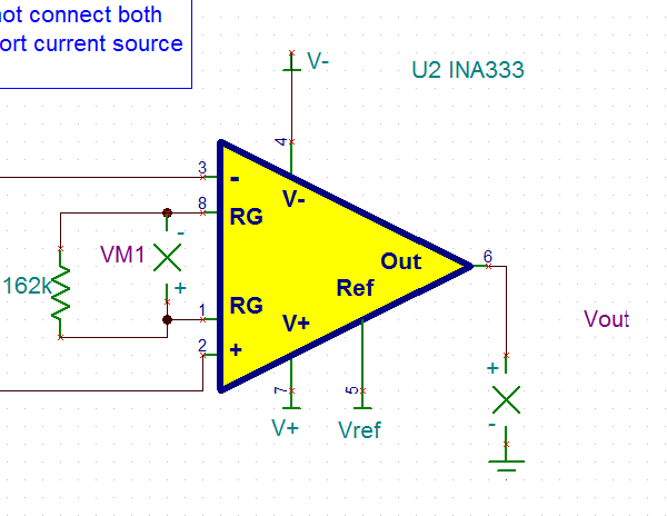
    The design of INA333 in Tina-TI and in the datasheet are different.

    Tina-TI : 

    Where Pin 2 is V+ and Pin 3 is V-

    and datasheet :

    where Pin 2 is V- and Pin 3 is V+.

    There is a mistake in one of them (I supposed that it's in the Tina-TI).

    Regards,

    Fabrice Péden

  • Hi Fabrice,

    The pin out shown in the datasheet is correct. Thank you for making us aware of the mistake with the Tina-TI model.

    -Tim Claycomb

  • hello Tim,

    I have the same electronics circuit, but i have some problem to undestand the result.

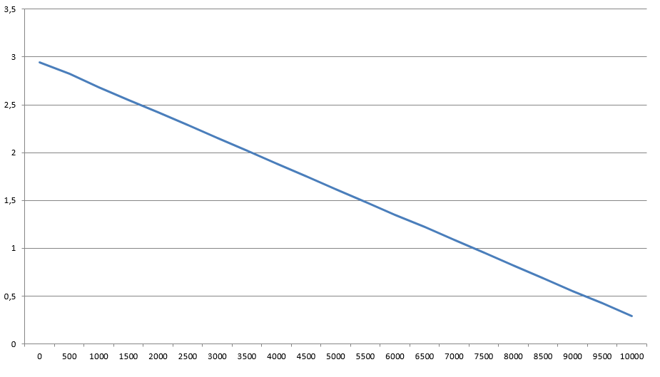
    If i look your result => Vin = 10V => Vdiff = 2.16V => Vout = 0V

    But if i try to calculate with Vin = 10V and Vdiff = 2.16V i found Vout = -1.5V (Vref =3V, Rg = 90.9Kohm, R1 = 100Kohm, R2 = 27.4Kohm and R3 = 107ohm)

    can you help to undestand my mistakes ?

    Thank you in advance

    Best Regards

    Malo

  • Hi Malo,

    Could you please share a copy of your schematic? I know it is similar to above but it sounds like you have changed a few things.
  • Hi Zak,

    my schematic is exactly the same and the measures on my electronic card are goods.

    But i don't understand your formula (i want to write the formula in my SW). When i try to calculate i don't find the good result => my curve is more sloping.

    I think one parameter is forgotten, but which one ?

    Best regards

    Malo Hénaff

  • Malo,

    I'm not sure what you are referring to. Do you mean you do not see a gain of 2.1 (1 + 100k/RG)? I will need more information about the issue you are seeing to assist you.
  • Hi Zak,

    Sorry, i have some diffficulty to explain my problem

    Exactly, i see a gain of 2.1. So, if i calculate with G = 2.1 =>

    Vout = ((V+) - (V-))*G + Vref

    Incase of Vin= 10V => V+ = 0V and V- = 2.15V => Vdiff = 2.15V

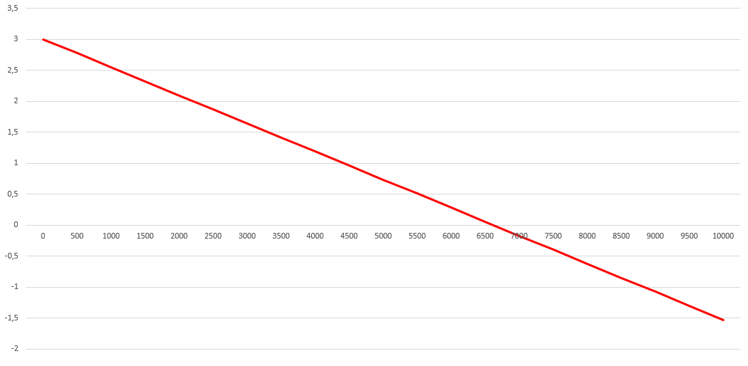
    Vout = (0 - 2.15)*2.1 + 3 = -1.5V

    if i look your curve with Vin = 10V, the result is 0V => i don't undestand why my result is different

    The blue curve it's texas instrument result, and red curve it's my result when i try to calculate.

    So i don't undestand the theoretical calculation. Can you explain me the theoretical calculation ?

    Best Regards,

    Malo

  • Hi Malo,

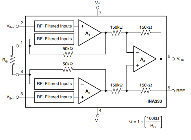
    Thank you for sharing this information, I understand the problem now. The issue here is that half of the INA333 is not actually operating in the linear region, so the gain equation differs than what we specify in the datasheet. Please refer to the following figure: 

    You can think of normal INA operation in the following way: Since A1 and A2 each want to drive their inverting nodes to the voltage present at their respective input pins, the same differential input voltage applied at the inputs is impressed across the gain setting resistor RG. The resulting current flows through each of the 50kOhm feedback resistors and forces the op amps to move their outputs to maintain the differential voltage across RG. 

    By grounding the positive input of the INA, you force A2 to slam as close as it can to the negative rail (about 30mV or so). This 30mV saturation voltage now becomes a constant reference at the input of the difference amplifier (A3). Now instead of moving to create the differential voltage across RG, the output of A2 is fixed. A1 will now act as a standard non-inverting amplifier with a gain of 1 + (50k / (RG+50k)). Now the equation for your output voltage becomes Vo = Vdiff * [1 + (50k / (RG+50k))] + Vref + Vsaturation. So even though you see a linear output, part of the internal architecture is operating outside of the linear region and consequently, you can not expect to see datasheet performance. While functional, I generally would not recommend operating the device in this fashion.

    Note, if you operated this circuit in dual supply, A2 would be able to swing linearly and the transfer function would match the red curve you predicted above. If you would like to adjust the design to remain within the linear operating region, this Common-mode vs. output voltage tool is very useful for visualizing the linear range of the INA for a given set of conditions:  

    I hope this helps!

  • Hi Zak,

    Thank you for all your assistance. Now i understand the calculation and i find the good result. I can use the good formula in my software.

    Thanks again,

    Best Regards

    Malo