This thread has been locked.

If you have a related question, please click the "Ask a related question" button in the top right corner. The newly created question will be automatically linked to this question.

About opa2227

Other Parts Discussed in Thread: OPA227
 Hello,dear sir or madam
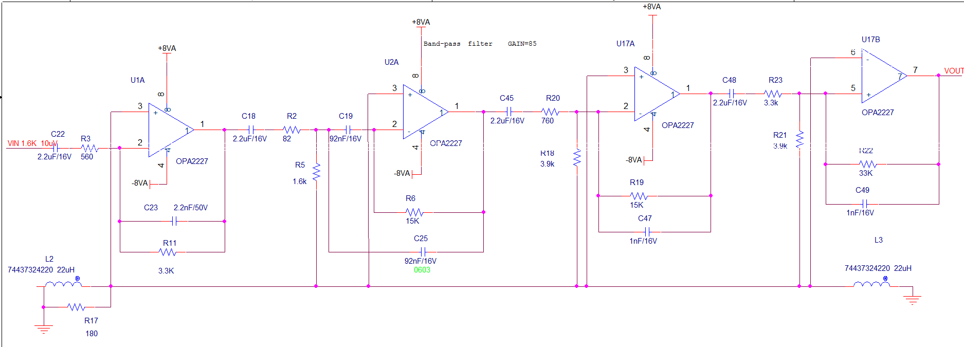
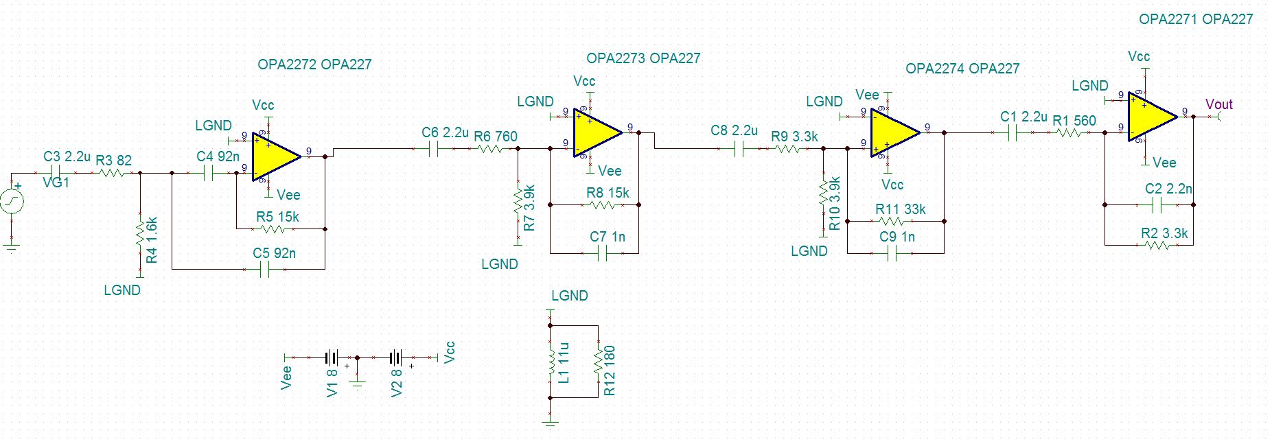
I need some help about op-amp opa2227.Situation is like that, I give the system one 100uV sine input signal, after 4-stageopa227 magnified 100 thousant times, the waveform jitters and amplitude changes.
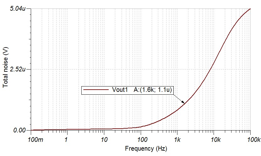
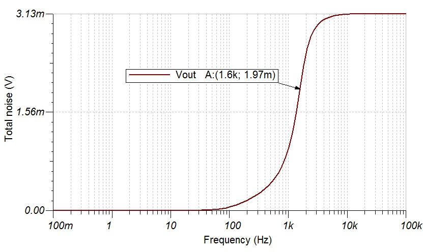
 I had simulated the circuit ,and it was correct when simulated.while the actual circuit can not work successfully.Tht output waveform  is as follows.Anyone could tell me what  happened about the circuit or the phenomenon?Tht output waveform  video is as follow,
  • Hello Bingtong,

    After reviewing the video and making some assumptions, I believe this may be a noise problem. However, I cannot be exactly sure unless a schematic is provided—please feel free to provide one.

    Assuming that your circuit is multistage with varying levels of gain, your simulation is correct, your simulation is not accounting for noise, 1.5kHz is within the bandwidth of the system, and your voltage supplies are sized so you do not violate any common mode or output voltage range limitation, I see 2 major possibilities for problems:

    • You did not account for the noise gain of the overall circuit
    • There is an issue with the equipment used and measuring the output

    For the noise gain of your circuit, remember that the noise gain can be different from the overall gain of your circuit. Noise of the amplifier is always measured at the noninverting pin of the op-amp. This means, if any of your amplifiers are put in an inverting configuration the gain of the noise will still be measured at the noninverting pin. This noise is gained throughout the system since each stage’s gain is multiplied to the previous stages. When you combine this fact with large resistor values in the feedback paths needed to generate the large gain of your system and voltage noise from each amplifier, you get significant amplified noise problems.

    Adding filtering to your circuit to limit the bandwidth (BW) around your desired frequency will greatly help reduce noise.

    You can learn more about noise, how to calculate it, and what is important to consider when regarding noise from the noise video series of TI Precision Labs.


    When probing the output, be sure that your oscilloscope probes are as close to the pins of the device as possible. Look at your function generator and oscilloscope without the circuit connected; if the noise floor is close to the amplitude of your sine wave (100µV) then it may not be possible get a clean output. If your frequency of interest is 1.5kHz, you may want to consider limiting the BW of your system and the oscilloscope BW settings to get cleaner results. Using connectors like BNC or SMA will usually offer better results than the scope probes since they can act like antennas for extrinsic noise—however this may not be possible with your circuit configuration.

    TI Precision Labs also offers a video about how to measure noise in the lab which offers many helpful guidelines like the ones shown here.

    I also encourage you to double check the simulation frequency response of your system and make sure that your output voltage at 1.5kHz is around 100dB. Also, I encourage you to make sure the voltage supply rails can support 10V of swing since the output voltage range of the op amp needs 2V from each rail (so a minimum of +/-7V on the corresponding supply).


    Best,

    Cole

  • Hello  Cole,

    Thank you for your guidance.I have checked the simulation frequency response of my system and make sure that my output voltage at 1.6kHz is around 100dB. Also, I make sure there  is no issue with the equipment used,measuring the output or supply voltage.My schematic  is as follow.

    I did not account for the noise gain of the overall circuit accurately.While,to reduce the effects of noise on the output,I put the second-level designed as a band-pass filter.The center frequency is 1.6KHz,and 3-db bandwidth is 200HZ.

    The distortion present at the stage 3,and it is worse at stage 4.

    Could you make sure the reason after reviewing the schematic and the video?

    Is there any way possible to result the question?

    Best,

    Bingtong

  • Hello Bingtong,

    Apologies for the late reply, I wanted to simulate your circuit and gather some insightful graphs.

    I would also like to say thank you for providing the schematic. In future E2E posts, feel free to provide a schematic to give us more information to help solve your problems.

    After reviewing your schematic and your changes, I notice there are a few more things to further reduce noise in your circuit. However, I think that it is important to point out that a 100µV (or 10µV like it says on your schematic) is comparable in magnitude to the noise that you will see in your circuit.

    Using TINA-TI a SPICE simulation software I was able to simulate your circuit and obtain the total noise and the voltage noise density curves. The first stage of your circuit alone with contribute 1.1µVrms at 1.6kHz like shown in the figure below.

    As a result, the noise will be coupled into the signal, gained up throughout every stage, and eventually corrupt the output. After looking at the video I am surprised that the problem is not worse.

    However, I do have some more suggestions for you to help you in your endeavor. I noticed that all of your gain stages are almost equal in magnitude. Traditionally it is better to put the higher gain stages first so the noise of subsequent stages contributes less to the output.

    For example, the figure below shows the total noise at 1.6kHz for your current circuit configuration.

    Taking note of the 2.33mVrms voltage-noise, I then arranged your circuit so the higher gain stages are first and obtained 1.97mVrms voltage-noise shown below.

    To build on this topic, you should try to put as much gain as possible in the first couple stages. I notice that your highest gain stage is 25.8dB which equates to 19.5V/V. If the OPA227 GBW product is 8MHz this means your effective BW is 410.3kHz when you realistically should have at least 1 decade above your frequency of interest (feel free to be more aggressive if necessary).


    In summary, I encourage you to front load your gain on the beginning stages and increase the gain on those stages. Amplifying signals this small will always have noise problems, but you can minimize those problems with these techniques.


    If noise continues to be problem, you may have to look into using smaller valued resistors that can accurately give you the gain you want, using low distortion C0G/NP0 type capacitors, and replacing the op-amp you are using with a lower noise model. This will increase the cost significantly.

    Additional Notes:

    I notice that you have resistors and inductors connected to ground in your simulation. I assume this is to model the trace inductance and impedance of PCB layout because they do nothing for your circuit otherwise.

    I also see that your last stage is using the noninverting pin for feedback; I would double check if this was intended.

    It seems like this schematic is bigger than what you showed me—which is fine. I would like to encourage you to look into decoupling capacitors near the positive and negative supply pins of the op amps to help reduce transient problems you may have.


    Best,

    -Cole