This thread has been locked.

If you have a related question, please click the "Ask a related question" button in the top right corner. The newly created question will be automatically linked to this question.

OPA2376 | V,os at VCM = 0V (single supply)

Other Parts Discussed in Thread: OPA2376

Team-

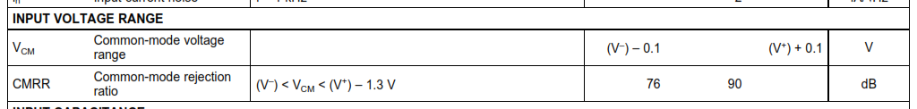
Fig. 23 of the OPA2376 data sheet indicates that V,os begins to degrade as V,cm -> 0V.

The data sheet spec's V,os for V,cm = Vs/2.

How much degradation of V,os can we expect when V,cm -> 0V?

Thanks, Best, S. Dunbar, AFA Colorado

  • I would like an idea of Ibias max with a temp of 70-75*C, but cannot interpolate from Figure 11.
    Is there any dependency of Ibias on Vcm?
  • Hi Steve,

    The change in offset voltage vs. common-mode is most prevalent in the upper common-mode voltages where the NPN input stage takes over to prevent phase margin and allow for a functional rail-to-rail input stage.  The common-mode rejection ratio defines the change in offset voltage vs. common-mode voltage and is valid over the region in question near V-.  Therefore the worst-case change in input offset voltage vs. VCM near the V- supply is 76dB or roughly 158uV/V. 

  • Collin-

    Understood about the V,OS at the upper end. We are specifically looking at the lower end.

    We would not think to apply CMRR to this otherwise DC precision offset parameter.

    If V,CM = 0V, then what is the degradation in V,OS? I'm not sure how to apply the 158 uV/V here.

    Thanks, Best, steve
  • What is Ibias max with a temp of 70-75*C? I cannot interpolate from Figure 11.
    Is there any dependency of Ibias on Vcm?
  • Thinking about this a little more using CMRR, if we go from V,CM = 2.5V down to V,CM = 0.0V, that's a shift of 2.5V.

    According to your analysis, V,OS must be degrading 2.5V * 158 uV/V ~= 400 uV.

    This would be far more than what is actually shown in Figure 23, no?
  • Hi Steve,

    Your calculations are correct for translating VCM shift to Vos shift using the CMRR specification. 2.5V * 158uV/V = 395uV. Keep in mind that all datasheet plots represent the typical behavior unless otherwise noted. Therefore Figure 23 was based on the typical specification of 90dB or 31.5uV/V, which would result in only 79uV of shift when moving from a Vcm of 2.5V to 0V with a 0-5V supply.
  • Hi Tim,

    The input bias current of a typical CMOS op amp is dominated by leakage current through the ESD protection diodes.  As a result the input bias current will double every 10C.  The typical input bias current is 0.2pA at 25C.  Moving from 25C to 75C, the input bias current will double 5 times (75C - 25C) / 10C = 5.  Therefore, the input bias current can be estimated to be 0.2 * 2^5 = 6.4pA.  Datasheet graphs represent the typical device performance unless otherwise noted and Figure 11 matches well with the calculation.  

    The input bias current will change minimally over the input common-mode range of the device.  Once the input common-mode range is exceeded the input bias current will increase significantly as the protection cells begin to conduct.

  • I need to worst case stack up of non ideal behavior to insure my design works across all devices and temperature.
    From above, Vos (25*C) is 25 uV. Shifted for temperature, gives 25 + 2uV/*C x (70-25) = 115 uV.
    Then I adjust for Vcm shifting (worst case), which is 158 uV/V, shifting additional 396 uV.
    Worst case Vos = 115 uV + 396 uV = 511 uV, correct?

    Similarly, for Ibias, starting at worst case of 10 @ 25*C, shifting to 75 *C = 10 x 2^5 = 320 pA, correct?

    Thanks,
    Tim
  • Hi Tim,

    The calculations for the maximum bias current are correct.  Your calculation steps for the offset voltage are correct, but you should use the 1uV/C specification for temperatures under 85C (see spec table below). So the maximum Vos due to temperature at 75C is 25uV + 50C * 1uV/C = 75uV, yielding an absolute worst-case situation of 471uV.

    That said, both of these conditions are unlikely to occur in a production system.  Devices with a single maximum specification are already on the far edges of the Gaussian distribution, making them rare.  A device that would display all of the maximum specifications is nearly statistically impossible.  This is because most maximum specifications represent at least a +/-3sigma distribution (99.7%), meaning only 0.3% of the entire population of produced devices have one specification at or above the maximum limit.  Devices outside the maximum limit are discarded.  Combining even two maximum specifications results in a +/-6 sigma type device or 1 in 500 million units.  Combining more maximum specifications results in an even more unlikely device. 

    So, while your results do predict the absolute worst scenario you could encounter using this device, the chances of you receiving such a device are very small.  Often specifications are combined using an RSS (root of the sum of squares) method to produce more probable results.

  • Hi Collin,
    Thanks for the clarifications.
    How about offset current. Does it vary with Vcm or Temperature? I don't see curves on this. Again, I'm operating close to Vcm = 0.
    Thanks,
    Tim
  • Tim,

    The input offset current change vs. common-mode will be similar to the input bias current and shouldn't change much over the specified common-mode input voltage range.

    Since the 25C typical and maximum input offset currents are the same magnitude as the input bias currents, it makes sense that as the input bias current specification begins to increase with temperature the input offset current has the potential to do the same. Keep in mind that most devices will behave close to the typical performance while other much less common devices may experience much worse changes if the input bias and offset currents were originally near the maximum specifications.