This thread has been locked.

If you have a related question, please click the "Ask a related question" button in the top right corner. The newly created question will be automatically linked to this question.

Incorrect OPA209 simulation

Other Parts Discussed in Thread: OPA209, TINA-TI

I am testing  current capability of op-amps (for the purpose of  component selection) by evaluating voltage swing to rails with simulation in Cadence/OrCAD PSpice.

I do it by sweeping through a current source at the output (at 75°).  For negative rail (and currents) the V2 is set to 0V.. However, I get 100% nonsense (e. g. output voltage beyond supply rails) with OPA209 and sometimes fails to run altogether 1

Green is supposed to represenr output voltage and red the swing.

The paramenter are transferred to model with

X^@REFDES %+ %- %V+ %V- %Vout @MODEL 

  • Hello Andrey,

    I've performed some output current vs. output voltage simulations in TINA-TI using the OPA209 model. Looking inside the model definition, I saw that the table below was used to create the output voltage swing characteristic. Linear interpolation is used for output currents between these points, so the model behavior is a good approximation of the typical amplifier behavior at room temperature.

    Iout (mA) Vout (V)
    0 Vs - 0.2
    30 Vs - 0.6
    50 Vs - 1.5
    64 Vs - 2.5
    > 64 current limit

    The simulation results matched this definition very well. My test schematics and resulting plots are shown below. I recommend modifying your test schematic in Cadence to use an inverting amplifier configuration with large value feedback resistors. This prevents the input voltage from sinking large currents into the part and helps with convergence. Also check the direction of current flow from your output current source. For sourcing current, you want the current arrow to point away from the OPA output, and for sinking current, you want the current arrow to point into the OPA output.

    The simulation circuit is attached below. Using our free TINA-TI simulator, you can verify my results by performing a DC transfer characteristic for either Iout_src or Iout_sink.

    OPA209 Claw.TSC

    Best regards,

    Ian Williams
    Linear Applications Engineer
    Precision Analog - Op Amps

  • Thank you for the answer.
    Inverting? Won't it work in non inverting?
    As for sinking, I simply sweep through negative current values.
    Alternatively you could just tell me, what is the voltage swing (difference between rail voltage and closest possible output voltage) to positive rail while sourcing and to negative rail while sinking at 1, 10, 20, 30, 40, 50 mA
  • Hello Andrey,

    Some amplifiers will work in a non-inverting configuration, depending on their input common-mode voltage range. The reason we use an inverting amplifier circuit is because the common-mode voltage is held at 0V, or mid-supply in single-supply applications. This allows us to drive the amplifier output to the supply rails without input issues.

    The OPA209, a bipolar amplifier, has an input common-mode voltage limit of 1.5V away from each supply rail. Therefore, we would experience issues (voltage clamping, performance degradation, etc.) if we applied the supply voltage to the input in a non-inverting configuration.

    According to the model, which is a room temperature simulation only, here are the voltage swing limits at the output currents you requested:

    Iout (mA) Vout_min (V) Vout_max (V)
    1 -Vs + 0.19 +Vs - 0.19
    10 -Vs + 0.31 +Vs - 0.31
    20 -Vs + 0.45 +Vs - 0.45
    30 -Vs + 0.58 +Vs - 0.58
    40 -Vs + 1.03 +Vs - 1.03
    50 -Vs + 1.48 +Vs - 1.48

    For more detailed information, please see Figure 22 in the OPA209 data sheet.

    Best regards,

    Ian Williams

  • Ok, I beleive I understood. So in non inverting configuration the output is effectively limited by common mode voltage spec before the voltage swing becomes noticable at ~50 mA (assuming |Vs-1.5| V input) .

    Is there a button, with  which i could accept the last answer?

  • Hi Andrey,

    Your understanding is correct. Thank you for verifying the last answer!

    Best regards,

    Ian Williams
  • Hello Ian-san,

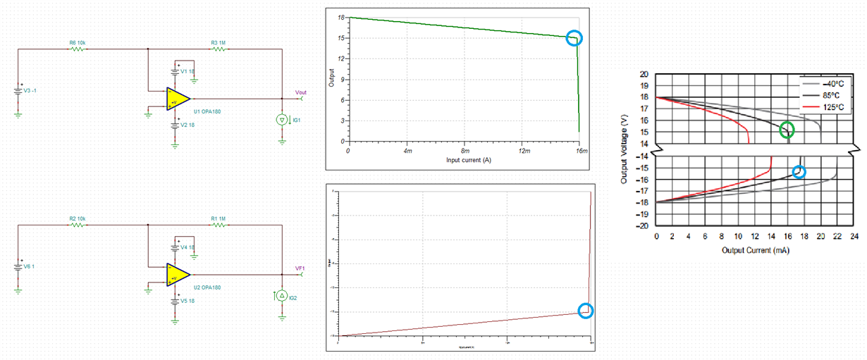
    I also want to know about how to simulate output voltage swing of OPAx180.
    Could you confirm whether TINA model of this device have table to create output voltage swing as well ?

    Best Regards,
  • Ryuuich-san,

    Below please see the circuit configurations used to determine the output voltage swing for the range of the output current.  The simulation matches very closely the graph in the datasheet - see below.  I have also attached the Tina-TI schematic so you may use to do your own simulation.

    OPA180 Claws.TSC

  • Lis-san,

    Thank you for your reply.

    I want to know how you can create attached figure.

    I want to simulate case of 50uA load current  in specific circuit.

    BR,

    Mahcida

  • achida-san,

    Iout of 50uA is almost zero load so the output will swing at least within typical 8mV shown in the datasheet - see below.

    You may also use attached schematic to simulate this condition.

  • Hi Lis-san,

    Do you know load current in case of RL = 10kohm in above parameter ?

    Best Regards,
  • Lis-san,

    I could simulate case of RL = 10kohm and confimed load current.

    So please close this thread.

    BR,