This thread has been locked.

If you have a related question, please click the "Ask a related question" button in the top right corner. The newly created question will be automatically linked to this question.

INA240internal input and feedback resistor

Other Parts Discussed in Thread: INA240

Hello,

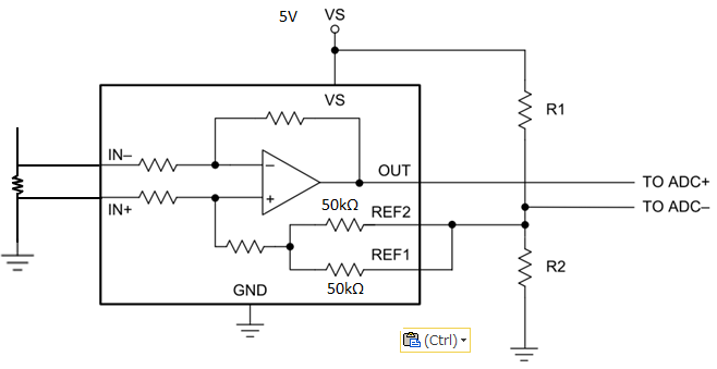
Customer is considering to use INA240A1 (20V/V) or INA240A2 (50V/V) with following figure.

This circuit use ADC- and ADC+ (differential ADC) so voltage change (error) of REF1/REF2 terminal will be cancelled so order of R1 and R2 should not be important, but customer wants to know the error of REF input voltage.

Datasheet has internal REF1 and REF2 value (50k ohm), but doesn’t explain internal input and feedback resistor value. So we can’t calculate the reference error caused by internal impedance and R1/R2


Please advise value of internal resistor or maximum leak current of REF1/REF2 terminal (INA240A1 and INA240A1) in case of above usage.


Best Regards.

  • Toshio-san,

    I'm assuming you are referring to the error between the reference and the corresponding value on output? According to the datasheet, the error due to the INA240 between your reference input and the output pin is .1% max (see below "reference divider accuracy"). However, you also need to configure the tolerance of whatever low impedance source you are using to drive the reference pin (in this case R1&R2). We recommend that you typically use a low impedance source to drive the reference pin, and the network of R1/R2 may cause issues in driving the pin. You will also introduce additional noise due to the ADC input loading the node as well. Just a heads up.

    As for the value of the internal components, I have reached out to design to see if we can obtain actual target values, but bear in mind that the values will be different based on which gain version is chosen. Also, I know from previous experience, that the tolerance on these resistors is pretty wide (around 20%), as the resistors are laser trimmed to match each other, not a target value. This includes the 50kohm resistors quantified on the datasheet, and may further complicate your R1/R2 setup.

    Hope this helps. Let me know what else you need.

    Carolus

  • Hello Carolus-san,

    Thank you for your answer.

    I understood that internal input and feedback resistor tolerance is pretty wide.
    Using method of figure 30, REF1 and REF2 error is cancelled using differential input ADC so Customer doesn’t need accurate resistor value.

    Could you please let me know the rough internal resistor value of INA240A1 (20V/V) and INA240A2 (50V/V)?
    (For example input resistor is several k ohm and feedback resistor is several ten k ohm.)

    Best Regards.
  • Toshio-san,

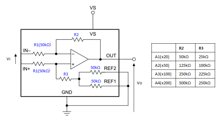
    Design came back with the numbers. For the resistor in the feedback line, the values are 50K/125K/250K/500K for the A1/A2/A3/A4 versions respectively. The shared resistor in the feedback path is 25K/100K/225K/450K for A1/A2/A3/A4 respectively. The resistors on the inputs are each 50K for all versions. Again, all of these resistors have a tolerance of +/- 20%, as they are laser trimmed to each other, not a specific value.

    Hope this helps.

    Carolus

  • Hello Carolus-san,


    Thank you for your answer.


    I want to confirm your answer.

    Do you say internal resistance is as follows?

    Vo=Vi(R2/R1) so Gain of A1 is as follows.

         A1 Gain = R2/R1 = 50k/50k = 1 (If R1 and R2 is 2.5k Gain is x20.)


    Could you please check the resistor value again?


    Best Regards.


  • Toshio-san,

    You are correct that the gain is 1. The INA240 is a two stage device (see section 8.2 of the datasheet). For all INA240 devices, the first stage creates a gain of 20, and then the resistor values I have given you complete the necessay additional multiplications for each part. For the A1 part, unity is all that is required by the second stage, as the gain from the first stage is already 20.

    Carolus

  • Hello Carolus-san,


    Thank you for your quick reply and I’m sorry for my many questions.


    I find “8.2 Functional Block Diagram” and first stage is “PWM Rejection Block”.


    Q1:

    Do you say that this “PWM Rejection Block” has gain of 20?


    Q2:

    My goal is to calculate error of REF1/REF2 terminal voltage using R1&R2 value in case of Figure 30.

    I got information of internal resistor but I can’t calculate error of REF1/REF2 terminal voltage because “PWM Rejection Block” is exists and R1 are not connected to external circuit directly.


    Please advise how to estimate error of REF1/REF2 terminal voltage caused by relationship of REF input impedance (leakage) and R1/R2. (Rough calculation is acceptable.)


    Best Regards.


  • Toshio-san,

    The output from the PWM network is aimed to be midsupply +/- 10*V_sense on each output. Therefore the common mode at the R1 resistors is Vs/2. However, this is not precisely trimmed, and we do not typically spec this, and as such we cannot guarantee it. The value does not matter. as the common mode is being removed by the differential input. With this value, the customer should be able to calculate the error at the reference output, but ultimately, why does it matter? They can find the nominal voltage at the ref output, but once they drive reference, which will propagate to the output pin, the error would be removed by their differential ADC setup. Let me know your thoughts.

    Carolus
  • Hello Carolus-san,


    Thank you for your answer.


    We understand that VREF error is cancelled by using differential ADC.

    We sets Vref=VS/2 and it is equal to ADC- input voltage and we wanted to know the error of ADC- voltage.

    Your answer can be used to calculate ADC- input voltage error.


    Best Regards.