This thread has been locked.

If you have a related question, please click the "Ask a related question" button in the top right corner. The newly created question will be automatically linked to this question.

INA301: Significant gain error

Part Number: INA301

Hi everyone,

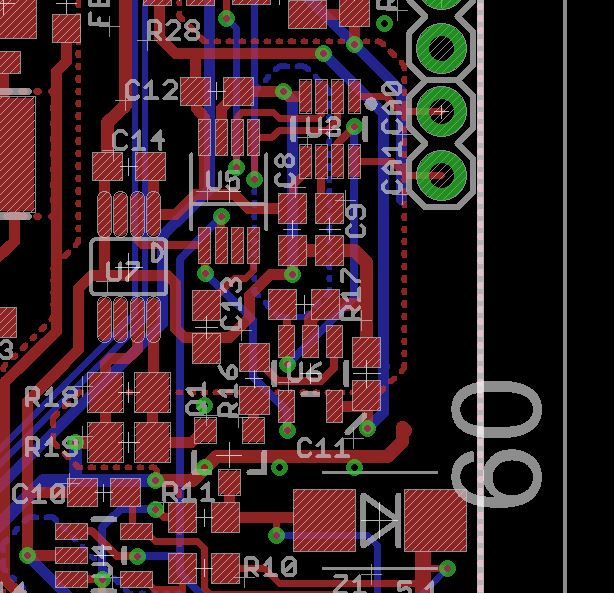
I am developing a precision current source using the INA301A1, but am running into some pretty significant issues.  One of my biggest problems is that the gain on the device is specified to be 20 V/V with a maximum error of 0.1% but I am seeing errors in gain as large as 9%.  

Has anyone had a similar experience or know what it could be caused by.  I have attached the schematic for the control loop.  The output of the current sense amplifier is feeding the input of the DAC. I have also removed the load voltage sense circuit since it contains an error.  I have removed the DAC and still get a significant gain error from the INA301.  I am also testing this with a 1k resistor across the load pins.

Thanks,

  • Dear Torkom,

    would it be possible to see a layout of your PCB as well? If you're seeing this much error, it might be a problem layout-wise on the board with respect to the INA301.

    A quick way to check this is to take a DMM and probe across the input pins of the device (NOT the shunt resistors). In fact, probe across the shunt as well and see what the difference between the two values is. If you see your error at the input side, then the error is due to issues on the input traces. I would recommend checking out video 13 from the link below on ways to combat those issues.

    https://e2e.ti.com/support/amplifiers/current-shunt-monitors/f/931/t/467332

    Let us know what results you see from this and we'll go from there. Hope this helps.

    Carolus

  • Hi Carolus,

    I have probed the input pins and they are exactly the same as the voltage across the shunt resistors.  I am interested in currents from 0 to 6mA with a resolution of 40uA, so I am using two 49.9 ohm 0.1% resistors in parallel.  I don't think that the trace resistance will have any significant contribution with such a high shunt resistance.  I have attached a photo of the layout for review.  The current sense amp is U7 and the shunt resistors are R18 and R19.  

    A couple more bits of information to help debug.  The supply voltage for the device is 4.5V.  It is provided using a switching regulator to boost to 5V from a 3.7V lipo and an LDO placed afterward.  There is a maximum ripple of 50mV pk-pk on the voltage rail.  The current is monitored by feeding the amplified signal into an ADC. There was still gain errors when the ADC was removed.  The analog and power grounds are tied together using a ferrite bead.

  • Dear Torkom,

    a few more things I noticed:

    - So to clarify, if you probe the voltage at the inputs of the device, and then probe the output of the device without a load, you are seeing aprroximately 9% error between the two? Have you tried mounting a new device to see if this replicates?

    - You say you are interested in a current ranging from 0 - 6mA, but what is your nominal current value? Are you running closer to the 6mA, or closer to the microamp range where your resolution lies?

    - On your schematic, it indicates you are using the A2 version of the part (50 V/V). Is this the case, or are you just placeholding for the package on your layout, and using the A1 part (20 V/V)? The reason I ask is that the offset voltage for each is different, and at such a small signal, this will have significant bearing on your measurement. From your notes, it looks like you are calling out the maximum offset of the A1, but I just wanted to double check.

    Carolus

    P.S. - Out of curiosity, why do you LDO the voltage back down to 4.5V from the Boosted 5V regulation?

  • Hi Carolus,

    I have probed the input pins of the device and the output pin and see *up to* 9% error. Sometimes the error is around 2-5%. For the tests I have been conducting, the current is between 1mA and 2mA. However, the project specifications require that I am able to to get resolutions of 40uA in the range between 0-6mA. The project is for a brain stimulation device so the currents can vary. There is no nominal value but I would say that its usually not at the very bottom of the range at 40 or 80uA.

    The schematic is incorrect. The device is actually an A1. I have not switched the device on the board, but I have 3 boards that have been assembled by my PCB manufacturer. All of my boards have a some amount of error. I have noticed that the error is a lot less with higher current values closer to 4.5mA.

    I used an LDO to have a cleaner source on my 4.5V rail. The regulator is a low noise regulator and I plan was to filter some of the ripple from the switching regulator (however this was not the case likely due to the high switching frequency of the switching regulator).

    Thank you,

    -Torkom
  • Torkom,

    Apart from the fact that we typically recommend a single shunt resistor (the kelvin connection of multiple resistors introduces error in the form of additional trace resistance), your layout looks fine. The fact that the error reduces as the signal grows larger makes perfect sense, and is probably the root of your problem. Given that you are measuring such small currents, it is more than likely that that the offset of the part and the input bias current are tainting your measurement.

    The maximum offset of the part is 125uV at the input side. Granted this may not be the true offset of the part you are currently using, but it can be present in any part, and should be designed to as a result. It looks like this error has been mitigated for the most part by your selection of such a large shunt resistor (50||50), as at 1mA, your input voltage would be approximately 25mV >> 125uV. I mention this, though, to keep it in mind moving forward.

    The typical input bias current of the part is 120uA. This current flows into both sides of the INA301 differential inputs, and therefore you will see the current entering the lower terminal flow across the shunt resistor. This is the equivalent of 3 LSB's by your resolution. With such a large shunt resistance, this is adding a significant amount of additional offset to your measurement (120uA * 24.95ohms = 3mV). This equates to up to 60mV on the output side. Again, this can be mitigated as you travel higher into the measurement range, but this has the possibility to dominate at such a low measurement range. Measuring 1mA, your ideal output would be

    1mA * 24.95 * 20 = .5V

    With the calculated offset from the bias currents above, you would be realizing an error of 12% before taking into account other uncertainties in the system.

    Finally, the gain error of the part is specified beginning at Vout = .5V. For signals smaller than this, the gain error of the part may change or operate outside the specified range, so you need to make sure that you design such that your minimum desired measurement outputs a voltage in the dynamic range of the part.

    I believe your issue is due to the balancing act of these issues present at the low end of the measurement spectrum. You can attempt to reduce the size of your shunt resistor to reduce the effects of the bias current, but as you bring the differential down, the offset of the part will become more relevant, and it will become more difficult to ensure that the part functions in the specified output range. You also have the option of stepping up to the next gain variant, which will provide additional design options to combat these issues.

    Hope this helps. Let me know if you need anything else.

    Carolus