This thread has been locked.

If you have a related question, please click the "Ask a related question" button in the top right corner. The newly created question will be automatically linked to this question.

INA333: INA333 input bias current return path

Part Number: INA333
Other Parts Discussed in Thread: OPA2170, TINA-TI, OPA376

Hi,

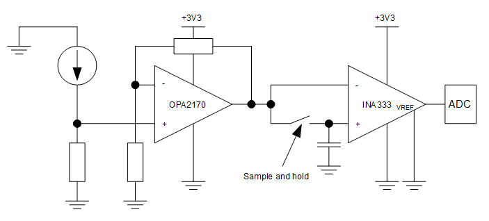
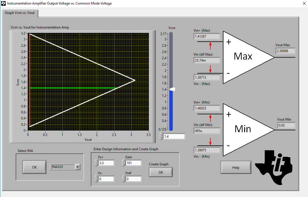
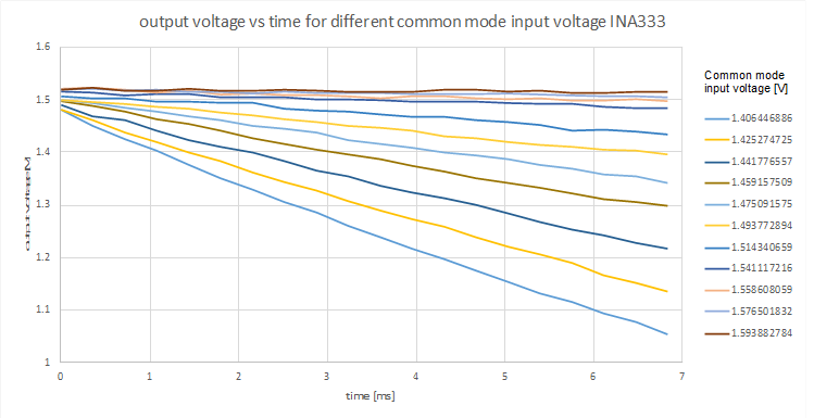
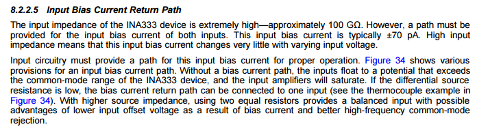
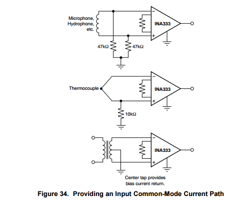
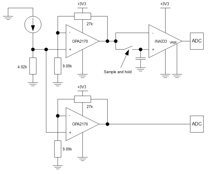
I have a question about the INA333 instrumentation amplifier bias current. My circuit looks as shown below. It is meant for measurements of very small current changes. The thing I have noticed is that the INA333 output voltage over time is very strongly dependent on the common mode input voltage within the common mode region that should be fine (see screenshot from the TI VOUTvsVCM tool). The sample and hold circuit simulations show the discharge of less than 400uV in 100ms, so this will translate (with 101 gain of INA333) to less than 40mV. In the plot you can see the voltage drop of more than 400mV within less than 7ms for input common mode voltage of ~1.4V. I came to a conclusion that the only reasonable explanation is no 'low impedance' path for the INA333 positive input. Could you please confirm that this behaviour is related to the bias current or do you have any other explanation? Since I cannot add a resistor in parallel to the hold capacitor the only solution seems adding an opamp buffer between the hold capacitor and the positive input of the INA333. Do you have any other idea how can I solve this problem? Thanks in advance for support.

best regards,

Maciej

  • Maciej,

    In order to prevent the input common-mode voltage change at the positive input of INA333, you must provide DC current path to ground - see text below.  Without it, a typical IB of +/-70pA will over time charge the sample and hold cap thus changing the differential input voltage; this in turn, will result in the output voltage drop as shown in your graph.

    Please be aware that INA333 is a chopper stabilized device which means that the actual IB is dominated by the short duration (few nano-second) current spikes at frequency of 125kHz coming from the closing/opening of the switches in its front-end.  The magnitude of the spikes may be in tens of nA and thus in order to prevent those current spikes from getting converted into voltage spikes across the input resistor, the value of sample and hold cap and dc path resistor must be chosen in such a way as to create a low path filter with the cut-off frequency significantly below 125kHz or be able to tolerate an increased voltage noise.

  • Hi Marek,

    thanks for your answer. I definitly think that I should provide the path for the bias current, but I would also like to understand the issue to make sure that it will be solved.

    To tell the truth I do not believe that the discharge of the hold capacitor is related to the INA333 bias current. The hold capacitor is the ceramic 10uF, +/-10%, X6S and it has 50MOhm minimum insulation resistance. 50MOhm at 1.5V would give you ~30nA of discharge current. I understand that the insulation resistance may be higher, but I doubt that it is 2 orders of magnitude higher than specified. 

    Even if we concider the worst case initial value of the capacitor and DC bias capacitance change (no temp coeficient, since the measurement is done in the lab at around 25 celcius degrees) then I expect to have at least 6uF of effective capacitance. The gain of the INA333 is set to 101, we see at least 50mV/ms output voltage change (for 1.4V common mode voltage), so it would translate to ~500uV/ms on the input. To achieve such discharge rate of 6uF capacitor you need a leakage current in the order of single uA. So I really doubt that the effect I see is caused by the discharge of the hold capacitor. I rather expect some kind of saturation in the INA333 caused by the high impedance on the positive input. 

    So the last question would be again: do you see any other way of making the path for the bias current than adding an opamp between the hold capacitor and the INA333 input? 

    regards,

    Maciej

  • Maciej,

    Your original question pertained to INA333 input bias current dc path but now it seems you look into potential causes of the excessive Vout shift.  I see several potential causes of the problem but the best approach to get to the bottom of the issue you see would be to monitor with a scope the voltage potentials at each of the input of INA333 instead of just looking at Vout.

    For one, you do not show what the initial voltages are at the inputs of INA333 and judging by the initial Vout of around 1.5V they are not at the same potential - are they within allowable level as shown in TI tool?

    Second, according to TI Vout vs Vcm tool, for the G=101 you use, there is a very narrow range of Vin inputs that are valid: from 1.387V to 1.412V (max Vin differential of just 25mV) and I’m concern you operate outside of the linear range.

    In addition, OPA2170 has the input common-mode voltage range specified from the negative rail up to Vcc-2V, which on Vcc = 3.3V single supply you use in your application means it’s valid only from 0V to 1.3V - you seem to operate above this range - at 1.4V

    You do not show the resistor values or close-loop gain around OPA2170 nor the current level you attempt to monitor – any variation of current level will directly influence your measurement.  I presume you do NOT make the measurement with zero initial current since this would attempt to drive the Vout of OPA2170 to ground – even though the input common-mode voltage may swing all the way to ground, its output is specified to swing linearly only witin 350mV above the ground (see AOL conditions).

    Btw, all OPA2170 specifications are defined with the minimum supply voltage of 4V while you use just 3.3V; also, why do you use general purpose OPA2170 with Vos of 2mV and then follow up with a high precision INA333 with max Vos of 25uV - if anything, the first gain stage should have higher precision than the second stage because the error of the first stage gets gained up at the input of the second stage.   

    Having said all of these, I must say I’m not sure why you need to use such elaborate circuit if all you seem to try to do is to measure the current level.  How about using one of our high precision, low voltage OPA376 in trans-impedance configuration as shown below?  I also attached the Tina-TI schematic so you may adjust the value of RF resistor depending on current level you try to measure.

    Maciek Circuit.TSC

  • Hi Marek,

    thanks for your reply. Actually the common mode range for linear operation of INA333 is around 1.6 - 1.7V if I want to have the output range up to 3V (by the way: 3V is the reference voltage of the ADC). But in the measurement data that you have seen the output voltage is around 1.5V, which means that the common mode range is much wider in this specific case: from ~0.9V to ~2.4V.

    1.387V and 1.4128V are voltages on INA333 inputs to achieve maximum output voltage within the linear range (2.6V) for the common mode voltage of 1.4V. At least that is what I understand from the TI tool. 

    Going back to the circuit: I have updated the circuit diagram with resistor values and the second OPAMP (I didn't include it in the first drawing because I thought it is not relevant, but it will give an extra insight). You can find the drawing below.

    I agree that OPA2170 was maybe not the best selection in this case (or at least I could have selected a better one), but if you look at important items: the gain of the OPA2170 in the non-inverting mode of operation is ~4 (R1 = 27k, R2 = 9.09k), so the common mode voltage for OPA2170 is between 0.35V and 0.4V - it is within the range of 0 - 1.3V. As far as I see in the datasheet the OPA2170 recommended minimum supply voltage is 2.7V (chapter 6.3), I didn't notice that all specifications are defined for 4 - 36V range. Regarding the offset voltage of the OPA2170: this is not a problem since I am using the SnH and amplifying the difference with INA333, the same offset is being added to both voltages (before and after SnH is asserted), so it shouldn't influence the measurement.

    Regarding the common mode voltage of the INA333: as you can see in the updated drawing I actually measure the voltage which is similar to the one on the INA333 input (within component tolerances) using the separate ADC - it is caluclated as (V0 + V1) / 2 where V0 is the initial voltage and V1 is the voltage after the change of the current I am measuring. 

    As you can see I want to measure very small changes in the current and I am not interested that much about the absolute values, that is why I am using the SnH with instrumentation amplifier. The first stage is only to achieve the good common mode voltage for INA333 since the current souce is limited voltage. Because any offset from the first stage is common mode for INA333 I have decided to reuse OPA2170, which is already in the design. I also thought about using the OPAMP in TIA mode before but since my current source is outputing positive current I would need to introduce the negative rail in the design, select different INAMP and so on. It just didn't seem to be worth it.  

    To sumiarize: I agree that the OPA2170 is not the best choice, but I think the circuit should work in principle at the moment and I still do not understand the voltage drop in time for certain common mode voltages. 

    regards,

    Maciej

  • Maciej,

    Just to make sure I understand what I am looking at in your Vout vs Time plots for different Vcm voltages.  Btw, are Vout vs Time plots actual measurements or simulation sweeps?

    Thus, you initially have the Sample and Hold switch closed and wish to measure a small change in the Iref (at the far left) – is this correct? Therefore, the idea is that right before changing the Iref current, you plan on opening up the switch counting that the cap at the positive input of INA333 will hold the input voltage steady for the duration of the measurement so you may measure variation in Iref – is this correct?

    If so, considering that your VREF is referenced to ground, I do not understand why the initial Vout at the output of INA333 is around 1.5V and not within 50mV of its negative rail as it should be with zero initial differential input voltage at the input of INA333.  This implies that the beginning differential voltage is not zero but rather around 15mV (1.5V/101) - please help me understand what am I missing here? Unless the cap you use is relatively small and the voltage gets messed up when the switch is opened.

    If the Vout vs Time plot is actual scope picture, please show the voltages at the inputs of INA333.