This thread has been locked.

If you have a related question, please click the "Ask a related question" button in the top right corner. The newly created question will be automatically linked to this question.

INA199: INA199 BAD gain

Part Number: INA199

Hello, 

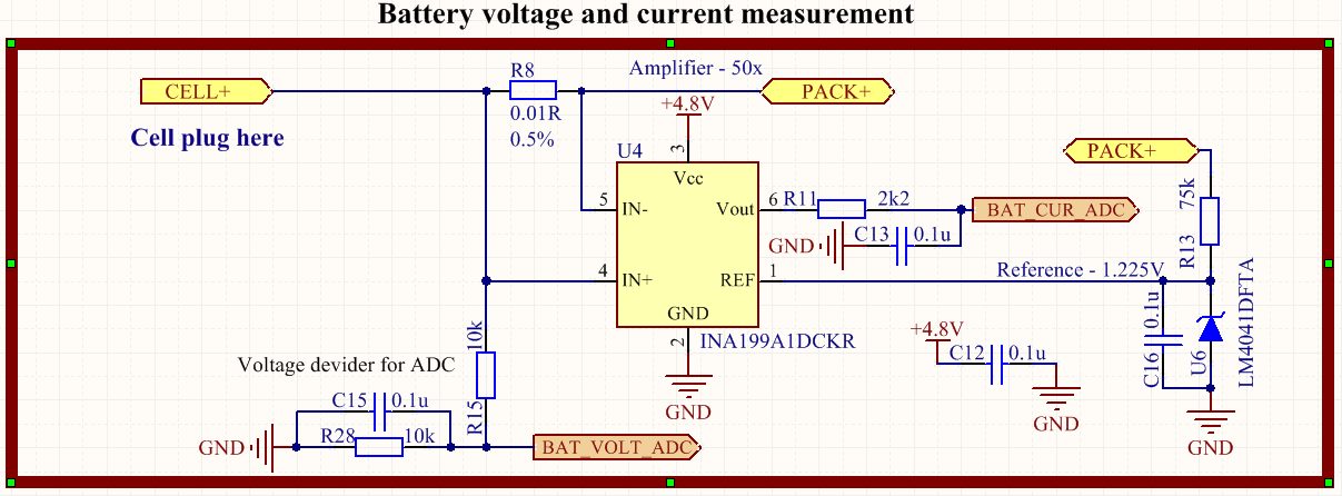
I have question about INA199A1DCKR and datasheet states that it's gain is 50V/V, but in my design I get 100V/V, maybe I do not understant something? My device trully is INA199A1, because I have checked device marking three times and it is written "OBG", that means it is 100% 199A1, not 199A2. I have attached my circuit . In both current flow directions INA199A1 amplifies 100 times, not 50 as stated in datasheet. I have 5 demo boards for prototyping and they all acts the same - can I trust that next devices 199A1 will have gain = 100, or it may be 50, 100, 200 depending on air conditions?

Thank You for help.

  • Hi Vaidas,

    Thanks for using TI E2E forums. The INA199A1 device gain is indeed 50V/V and this is not dependent on air conditions. You won't get gain of 100V/V from a A1 device there is something else happening due to the schematic configuration right now.  

    To understand what is happening I recommend you probe the Vshunt across the resistor and also at the INA input pins and Vout. Probing across the shunt resistor is typically the first thought. But if there is excess current flow for any reason through the filter resistors, this voltage could be different from the voltage at the input pins. Let's start by this readings and I will provide instructions for further debugging after this. 

    Video Session 14 from our Current Sense Training Video series explains where to probe for this type of debugging. 

    Regards,

  • Hello,

    thank You for the answer, but the problem, that I have measured everywhere where I could, before posting here. I am connecting just +4.8 and pack voltage - no current is flowing through R8 resistor, Vout is stable = 1.225V, the same as reference, then I connect this circuit in normal working state - current is flowing through R8 to one direction - voltge between 4 and 5 pin is 0.01V, I get ~2.225V on Vout pin. The same situation when current is flowing vice versa - I get ~10mV (different sign) between 4 and 5 pin and Vout~0.225V. Can You tell me where else I can probe? Reference stays stable all the time, multimeters internal resistance is >1MOhm, no other capacitive or resistive loads are added...

    P.S. I have watched video and everything is intuitive and I have measured the same way as in video.
  • Hi Vaidas, 

    Thanks for double checking for us. You are correct, with a 10mV Vshunt and 1.225V reference you should not be seeing 2.225V in Vout. At this point I would like to provide faster support by getting some of your parts here for me to test them on the lab. 

    Please send me an email to mayrim.verdejo@ti.com so I share my Mailing Address information. In this email, can you also let me know where you got this parts from? From a distributor? TI samples? Would you have any lot information?

    Regards

  • Hi Vaidas,

    Any update in this issue? Did you figure it out or you still need our support? I have not receive further info from you. Let me know how I can help.
  • Hello Mayrim, 

    no new updates on this issue, as it is just very small part of our project, as quick around we calibrate shunt regulator on first startup and that is it. After some time I will come back to this issue.

    We've bought these parts at Farnell and do not have any lot information. As this our product is just in early testing stage, it will not be difficult to change this part, just wanted to be sure that I am getting wrong results, that's why I posted this topic.

    I have attached layout. We are measuring really small currents, 1A, maybe a bit more, so I would guess it should not be really big problems in layout, because track resistance could not be comparable to shunt resistor... I understand if I would design current measurement for 100A, there would be difference to which resistor part to connect track, but now current density is really low and there is no any chances that there would be any voltage drop between shunt resistor different parts of pads (in my design, I take voltage from the center of pad)...

  • Hello,

    any updates on this issue?

    I'm having a similar Problem (also the 50V/V Version) - but only for a voltage output > VRef. For a current flow which result in an output smaller than VRef, the results are correct.  

  • Hi,

    Can you please help me understand your setup and results?

    Please share your schematic and application conditions: Vcm, Vs, vref, Rshunt, I load and your measurements at the input pins of the device (Vsense: differential voltage between IN+ and IN-). Also, the Vout you are seeing in that condition.

    Regards,