This thread has been locked.

If you have a related question, please click the "Ask a related question" button in the top right corner. The newly created question will be automatically linked to this question.

TINA/Spice/LMH7322: Latch enable clarification for LMH7322

Part Number: LMH7322
Other Parts Discussed in Thread: TINA-TI, , THS3202

Tool/software: TINA-TI or Spice Models

Based on spice simulation

I have designed my board around LMH7322 with following schematic

But output of board is not changing. Now I suspect that latch is not enabled. Because LE and LEB connections are swapped in EVAL schematic.

Simulation also works if both LE and LEB are connected to ground but on board situation remains the same and we don't get the output.

Please confirm the issue if there is a problem with spice model supplied. Will it work if I swap the connection of LE and LEB.

  • Sorry, I have checked the eval board its same as my schematic, But still the problem is that I am getting fixed output no change is taking place. Is there any way that I can confirm if IC has gone dead. I can't think of any other reason as output voltage levels are also as expected, 1.4V and 1V.
  • Hi Purnendu,

    Comparing the TINA-TI schematic with the EVAL schematic, it looks like the VTH connection should be on the IN- input (which is for the reference voltage or Vref) and the 49.9-ohm resistor to GND should be on the IN+ input (input signal to be compared with the Vref).

    With the EVAL schematic, if the VTH is at 5V (as used in the TINA-TI schematic) the IN+ will be at 2.5V (assuming 0V at the THS3202 outputs). For a 2Vpp input signal at IN+ centered around 2.5V and Vref of 0V at IN-, there is no way that the voltage at IN+ will transition below IN-. As a result, the output voltage will always be fixed with Q at 1.4V and QB at 1V. I think you can verify this by connecting NEG1 in the EVAL schematic to the same DC voltage as the IN+ pin and see if the output transitions.

    Best Regards,

    Rohit 

  • Just to clarify, VTH in the designed schematic is -5mv to -90mV variable, staying below IN-, and only goes up when the signal arrives (200mV peak).

  • Hi Purnendu,

    What is the NEG1 input voltage connected to? Have you tried to apply just DC voltage at the inputs to see if the outputs change state? I think the LE and LEB circuit schematic is correct. Have you tried to probe the THS3202 on an oscilloscope to make sure you are getting the right signal levels at its output?

    Best Regards,

    Rohit

  • 6560.Resonant Filter Board design.TSCCan I hijack this thread?? I am having trouble with the output of this part as well! I can't even get the simulation to work!

  • Hi Xavier,

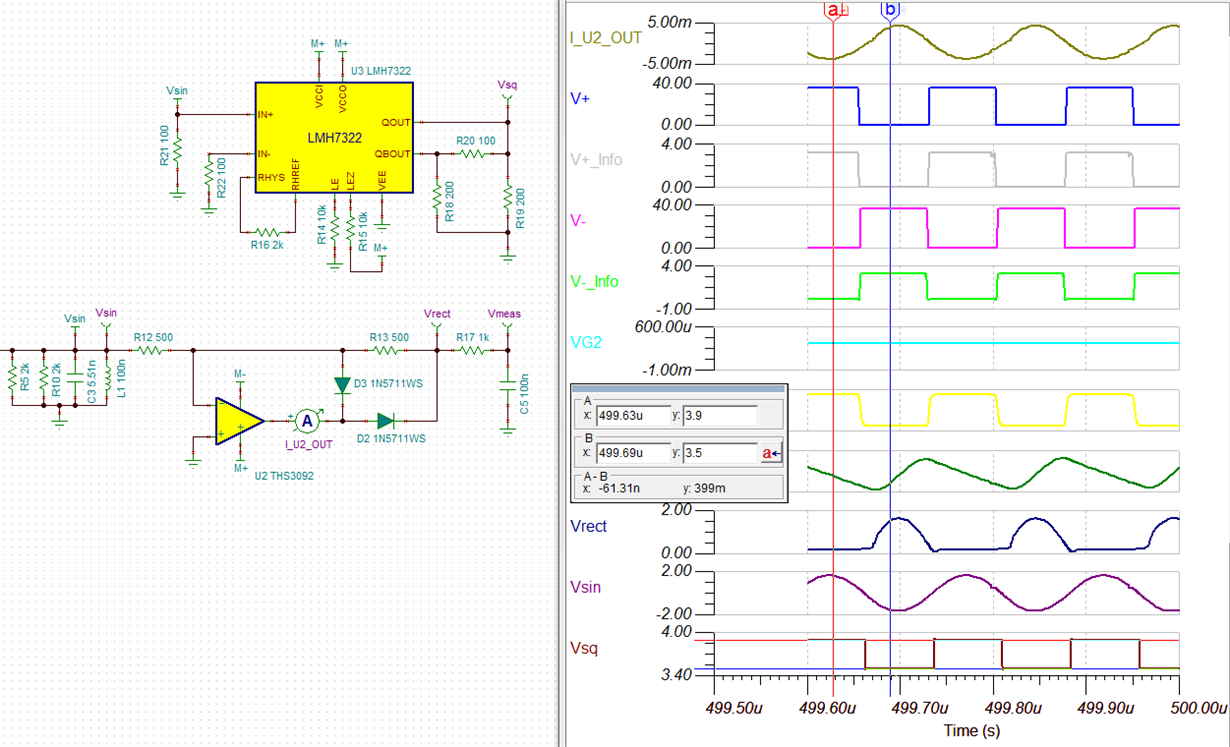
    I have attached a slight modification to your LMH7322 circuit which should toggle the LMH7322 outputs based on your inputs. Attached TINA-TI circuit for the same:7853.6560.Resonant Filter Board design.TSC

    Let me know if this works.

    Best Regards,

    Rohit

  • Hello!

    Thank you for the assistance! The change it looks like you made was adding a 100 ohm shunt to the inputs of the comparator? Is that necessary? and does it have to be 100 Ohm? 100 Ohm in parallel actually, rather severely, inhibits by resonant filter. Would it be ok if I used 10k or 5k instead??
  • Hi Xavier,

    It is recommended to have some termination at both the inputs. It does not need to be 100ohm. It is possible to use 10k termination instead of the 100ohms, but if the signal is high frequency then the line termination needs to be adjusted accordingly. I think in your case because your signal frequency is around 7MHz, you should be able to get by with 10kohm termination.

    However, I think the change responsible for the output to toggle seems to be the output pull-down resistors. I changed those from 82-ohms to 200-ohms because it seemed like the output was loaded heavily to the negative rail (VEE).

    Best Regards,

    Rohit

  • Wait... I just realized on your simulation that the LMH7322 is only toggling between 3.9 and 3.5... why isn't it doing the full range of 5 to 0?? Is it not supposed to?

    5 minute later Edit: Dammit I just realized how the RSPECL outputs work. I can't use this part. 

    10 minute later Edit: Small bit of frustration that it doesn't specify the RSPECL output levels explicitly EXCEPT for in diagrams which is very easy to overlook. 

    12 minute later Edit: I found where it specifies it... VCCO-1.1V and VCCO-1.5V.