Hello. I'm using the TL972 as a two stage bandpass filter with high gain. The bandpass filter is centered at 10kHz. My problem occurs when I turn on and off the emitter quickly, say at 2kHz (therefore five 10kHz pulses are sent per transmission). The output of the two stage filter behaves as expected during the on time, but once the transmitter is turned off, the output of the op amp goes to zero for 500us, then spikes up to Vcc (3.3V) for 500us, before settling down to the Dc bias (1.0V). As I'm modulating the 10kHz signal at 2kHz to be used in optical communication, this spike in op-amp output voltage is undesired as it causes false '1's to occur. Furthermore, the output of the first stage does not have this behavior. I'm unsure if this is instability, or the op amps response to a step function.
The image below shows the transmitter (blue) and output of the second stage of the op amp filter (purple). Time scale: 500us/div; vertical scale 1V/div for both channels. The large purple spikes at t=0 and t=2ms are the undesired spikes causing false '1's.
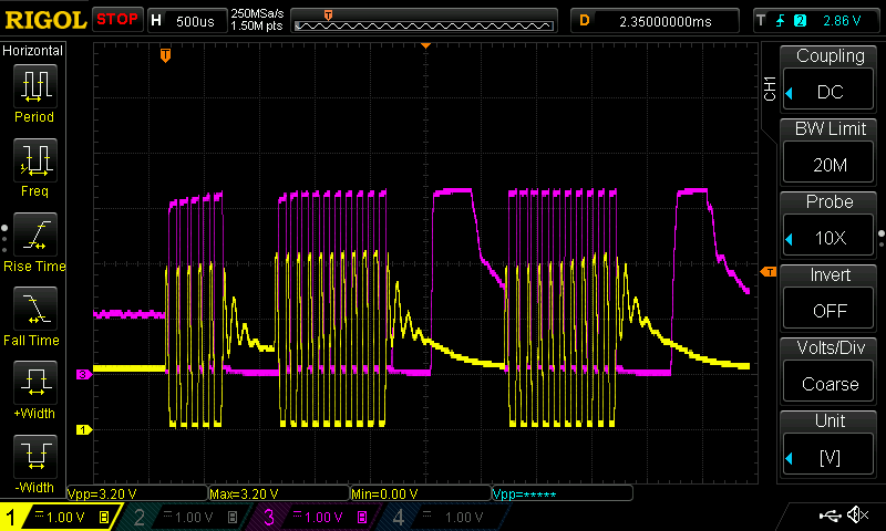
The image below shows the output of the first stage of the op amp filter (yellow) and output of the second stage of the op amp filter (purple). Time scale: 500us/div; vertical scale 1V/div for both channels. Notice how the output of the second stage is very different from the output of the first stage during periods the transmitter should be off.
Can someone help me understand the cause of this issue and how it can be alleviated? Below are snapshots of the schematic. Notice how 1V0 is created with a simple voltage divider. What are the reasons this should go into a buffer to be used as a reference?
Thank you
-Rob


