Other Parts Discussed in Thread: THS1206,
Hello Forum,
I am trying to use opa 836 as simple non inverting amplifier but unfortunately im facing some troubles in measurement with amplifier...
Input range : 100 micro volt to 2 volt
output range 1.5 to 3.5 volt to drive ADC THS1206
Vref available with on ADC board is 2.5 volt .
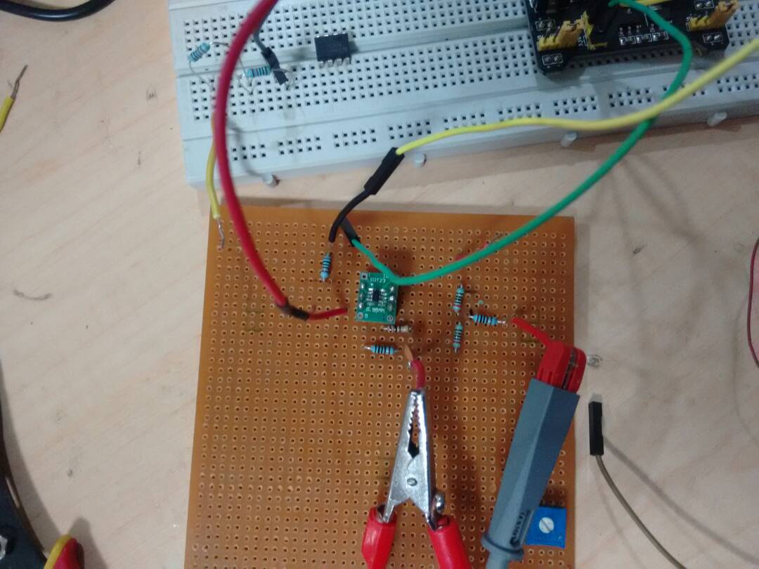
kindly find attached files of circuit diagram.
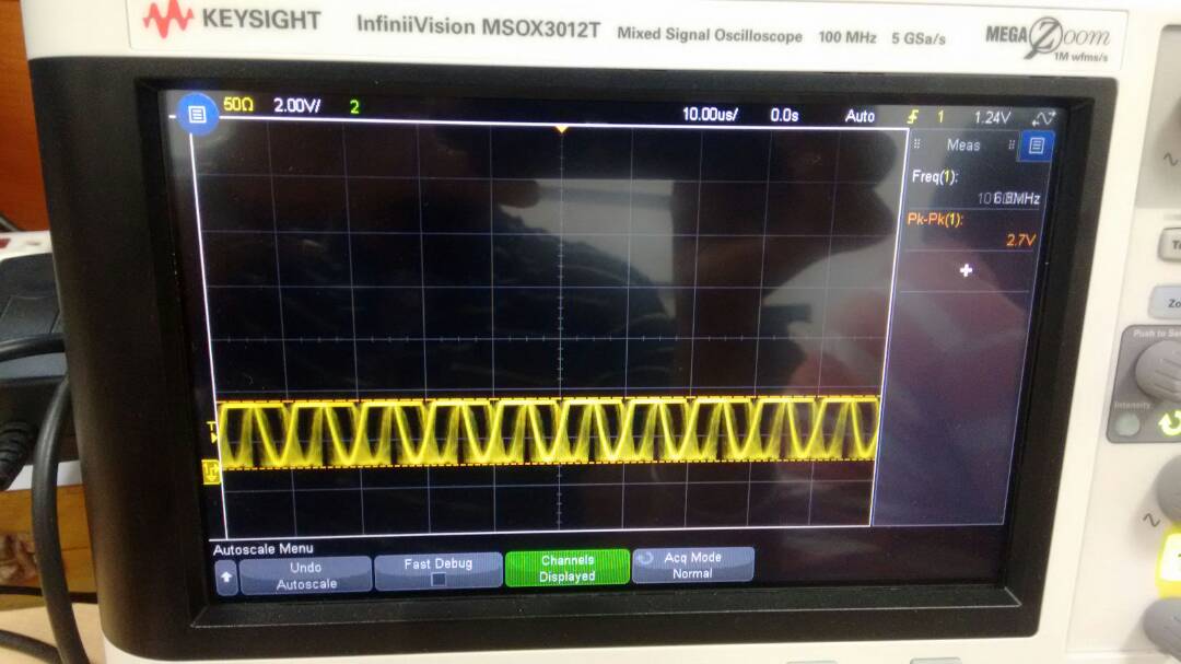
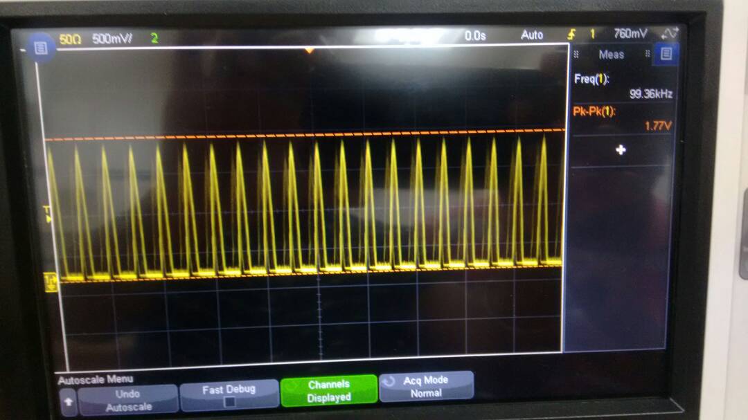
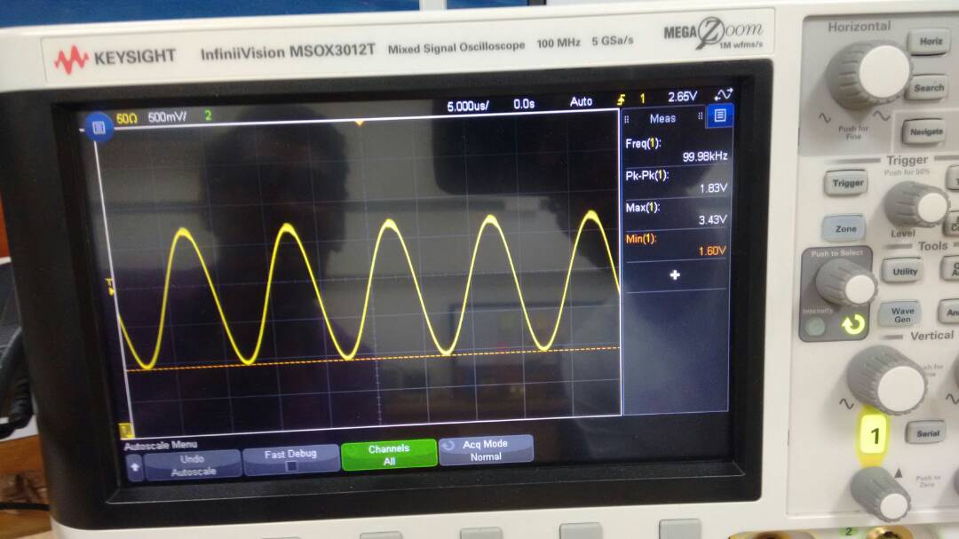
I have tried with the circuit given in data sheet fig 72 it's working fine for frequency range 1kHz to 1MHz but as I increase signal amplitude from 1 to 2vpp it's clamp the maximum level of output and shows 1.65 vpp so I have observed around 350mv loss in signal. As the gain is 2 it should show double the applied signal. I have also checked it with out applying Vref it's shows the same result that is clamping in signal.
please help me to tune the amplifier for mentioned CIRCUIT i/o RANGE.