


Part Number: INA333
Other Parts Discussed in Thread: OPA333, OPA330
Hi all,
Recently I have been debugging my circuit which is meant to amplify EEG signals from mice,
but I have encountered a problem with the INA333 chip (used as the first stage amplifier in a two stage amplifier design) that I can't seem to be able to fix so
would really appreciate if I can get some help.
Below is the schematic for the first stage of the AFE part of the circuit.
Model in TINA and simulation result when using a sine wave signal of 10mVpp at 100Hz:
The gain of the circuit is 100 and the INA333 is biased at half supply at 1.4V (Vref).
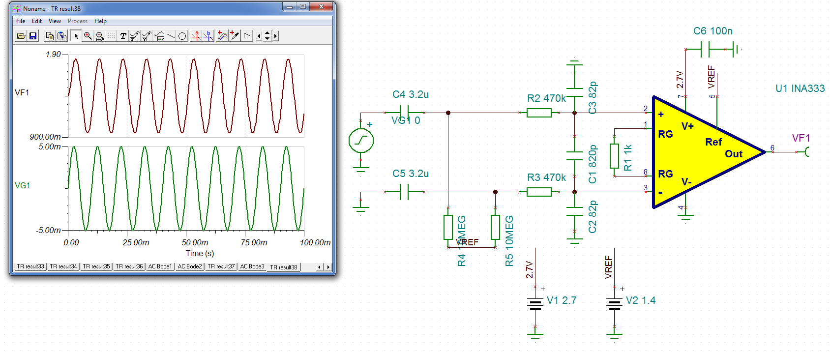
The AC response:
BandPass 0.005 to 200Hz ( overall the system system should be a 4th order bandpass from 0.01 to 150Hz so the first stage is designed to take into account the shift in cutoff frequencies due to cascading)

However when I test this circuit in the lab I do not get the same result. Instead of the output swinging from 0.9 to 1.9 I (centered at 1.4V) I get an output that goes from
0V to around 300mV. And this is due to the presence of a negative DC offset of around -16mV between the inputs.
Since then I have been been trying to work out what was causing this DC offset and I think it is due to the input bias current not having a return path due to
the resistors R4,R5 being too large. The reason I suspect this is as soon as I add resistors of 100K in parallel to them I get the output to be similar to the simulation result.
If I add the resistor only to R4 then the output goes to ground in a couple of seconds which I am taking it to be due to the accumulation of charges at the negative input.
If I add the resistor only to R5 then the output goes to positive rail in a couple of seconds which I am taking it to be due to the accumulation of charges at the positive input.
I was told that the offset could be due to the resistance of the capacitors C2 and C3 forming a voltage divider with R4 and R5, so I removed capacitors C2, C3 and C1 as well for good measure. But that did not affect the output.
After that I removed capacitors C4 and C5 and let Vref to be the input to both inputs of the amplifier, even that did not affect the output( ie it was still 0 to 300mV), it was only when I reduced the resistance of R4 and R5 (ie adding parallel resistors to them) the output became similar to the stimulation result.
So my problem is this, is 10Meg too large as the datasheet specifies a max DC biasing current of only 200pA. How do I calculate the maximum resistance allowed?. An easy solution to this problem would to reduce the resistance however this would reduce the input impedance of the circuit and I need the input impedance to be 1Meg or preferably 10Meg as the source impedance is quite high. So it there a better solution to this problem?
Sorry if the problem seems trivial as I am quite new to circuit design so I would really appreciate any help.
Thanks in advance!

