This thread has been locked.

If you have a related question, please click the "Ask a related question" button in the top right corner. The newly created question will be automatically linked to this question.

LM321: Why my LM321 output can't approach GND?

Part Number: LM321


Dears,

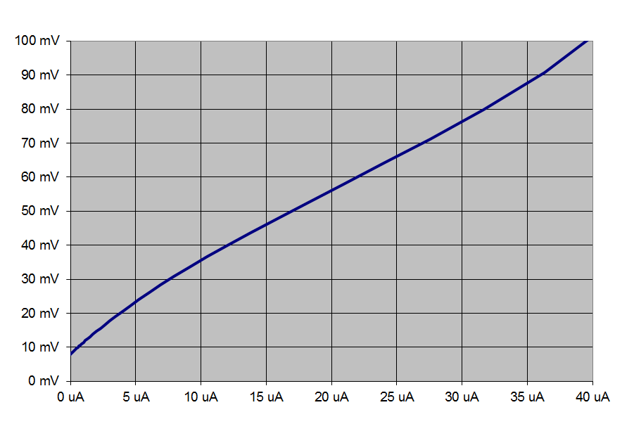
I used LM321 to design a difference input amplifying circuit, when the input is about 0V, but the output can't received the datasheet rating, When the input oV~2.4mV,the output is 40mV, but the datasheet is 20mV. whether is relation with the PCB layout or other design parameters? Could you kindly give me some sugeestion? Thanks!

My SCH as below,

  • Hi Jacking,

    I believe that the behavior the circuit exhibits does not relate to the output swing. It is probably not a dc offset issue either. Too that end, I would expect the dominant voltage offset source to be the internal voltage offset of the amplifier. However, it would only result in an output referred offset of about 21mV maximum.

    Rather, the offset might be due to a fairly weak output stage of the LM321. When the output voltage is approaching 0V (i.e the input voltage is close to 0V), the amplifier can only sink some 10s of uA (see figure 4 in the datasheet). Now, if your load is not connected to ground, but a positive voltage, the amplifier might have to sink more than that and the output voltage will be undetermined.

    I hope this might help you straighten out the problem.

    All the best,

    Gustaf

  • Dear Gustaf,

    Thanks for your detail reply.

    I have some confuse about the output sink current, the actual circuit is not floatt, you can refer the circuit. I want to konw what about the output voltage(minimun achievable) when the input is 0V. Thanks!

    Best regards!

    Jacking

  • Dear Gustaf,
    About the LM321 problem, could you give more suggestion for me? Thanks !
    Best regards,
    Jacking
  • Hi Jacking,

    The minimum achievable output voltage will depend on the power supply levels, loading of the output stage, the dc offsets (Vos, Ios, CMRR, temperature drift etc) and the output voltage swing, and will never be lower than the latter.

    Considering Figures 4 and 5 in the LM321 datasheet, it seems to me as if the loading of the output stage is causing these offsets. If this is the case, I would expect you to see an improvement if...

    ... you change the common mode voltage as referred to the supplies. You will then be able to come closer to the minimum achievable output voltage. You could verify this by trying a dual supply configuration.

    ... you add a positive bias voltage to the non-inverting pin of U30. Then your output would settle close to this voltage if 0V is applied to the input, since the transfer function changes to Vo = R180/R176*(Vp-Vn)+Vref.

    Kind regards,

    Gustaf
  • Jacking,

    The sinking current needed to support feedback resistor R280 is the reason for higher VOL. With only a 10k resistor to ground and no other loads would require no sinking current at all. Note that 0uA is less than 20mV

    Here is data from a similar output structure. Even a little sinking current can elevate VOL.

  • Dear Gustaf,

    Got it, Thanks very much!

    Best regards,

    Jacking

  • Dear Ronald Michallick,
    OK, I'will try do it, thanks!
    Best regards,
    Jacking