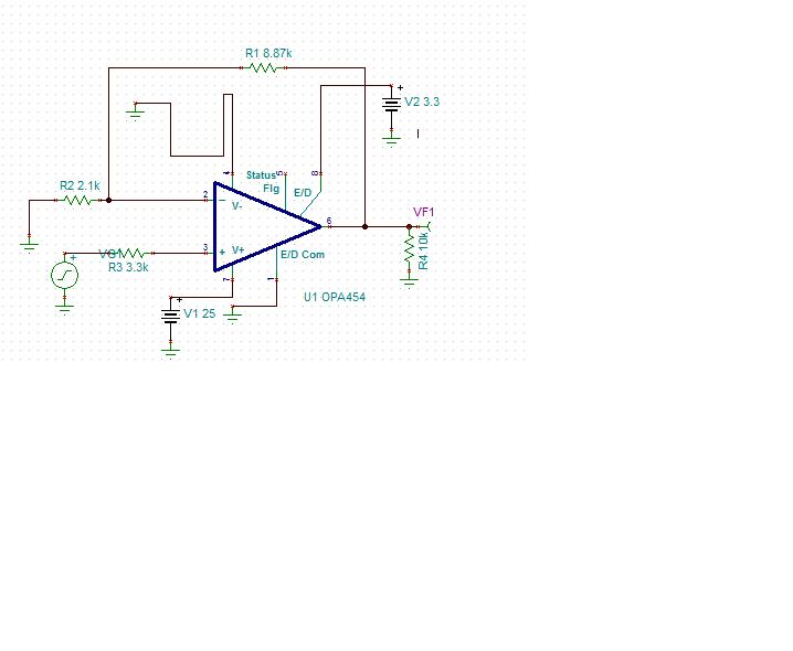
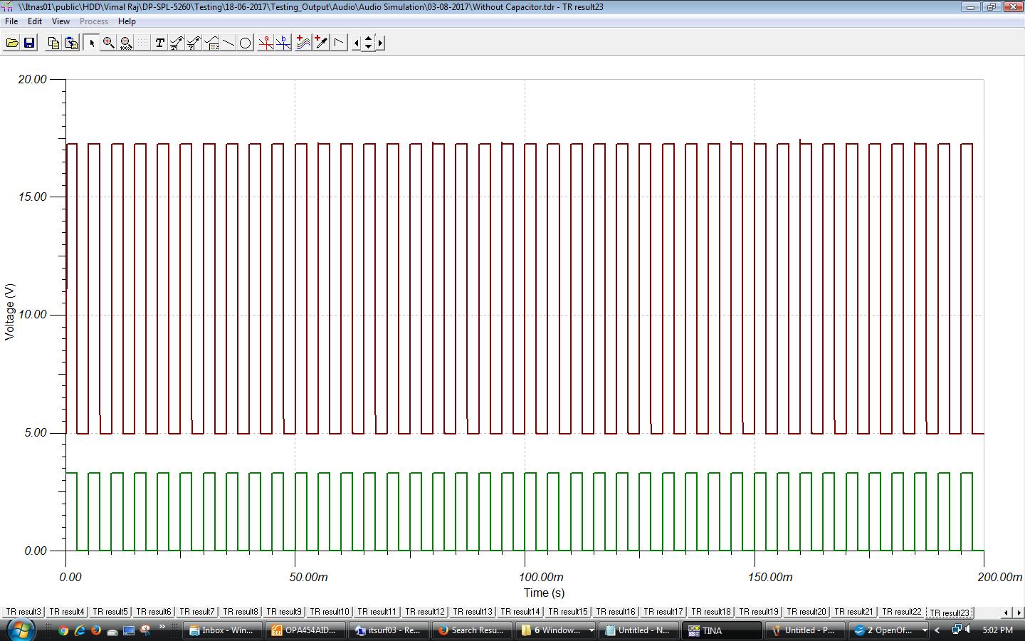
Part Number: OPA454
I used OPA454 OP-AMP in one of our design, The output of OP-AMP is having 5V offset WIth 12Vpp but i want 17Vpp output based on that I'm configured the gain values . Why this Offset comes in output
This thread has been locked.
If you have a related question, please click the "Ask a related question" button in the top right corner. The newly created question will be automatically linked to this question.
Part Number: OPA454
I used OPA454 OP-AMP in one of our design, The output of OP-AMP is having 5V offset WIth 12Vpp but i want 17Vpp output based on that I'm configured the gain values . Why this Offset comes in output
Hi Vimal,
You haven't provided us enough information about your OPA454 application circuit for us to make an assessment. Please provide the circuit shematic, supply information, details about the input signal and output load conditions.
Regards, Thomas
Precision Amplifiers Applications Engineering
Hi Thomas,
I attached the Schematic circuit, In circuit Supply V2 = 3.3V , VG1 = 3.3V, 400 Hz Pulse. Rin = 2.1K (in circuit it was wrongly mentioned as 1.1K) , Rf = 8.87K
Simulation output (Before Capacitor) is having 6V offset with 11Vpp voltage . Why this 6V offset comes at output.
Simulation output is also attached for your reference.
Regards,
Vimal Raj A
Hi Vimal,
You are driving the OPA454 enable/disable (E/D) pin with the 0 to 3.3 V, 400 Hz generator. The OPA454 output will provide normal linear amplifier operation when the E/D pin is high, 3.3 V, and then the output will become disabled when the E/D pin is low. In the disabled state the overall amplifier operating current drops to a very low level and the amplifier's output appears as a high impedance. It is then in power-down mode and the output node can be moved to whatever level is dicated by whatever the circuit configuration presents in that mode. In this case, the 2.2 uF capacitor has a dc level on it and that prevents the OPA454 output from moving down to zero, or near zero, volts. The minimum level it drops to with the 400 Hz E/D toggle rate is about 6.5 V. If the pulses cease the capacitor is eventually discharged and the output voltage drops to a level closer to zero.
Below, I show a TINA simulation where I have added a pull-down resistor to the OPA454 output. A transient analysis comparison is made with, and without, the resistor (R5) in the circuit. See Vo1 in particular for the dc output level. It can be seen that when R5 is in place the 2.2 uf capacitor has a lower resistance discharge path and the output voltage moves much closer to zero volts.
Regards, Thomas
Precision Amplifiers Applications Engineering
Hi Thomas,
As per above explanation, 6.5V offset occurs at output due to the 2.2uF capacitor, But i simulated the OPA454 opamp without capacitor & 400Hz, 3.3V Pulsed input , In this case , 12Vpp output comes with 5V offset. As per datasheet, Voltage swing range is given as V- +1 V minimum .
Kindly clarify the why the 5V Offset occurs at output.
Herewith I attached simulation results for your reference.
Regards,
Hello Vimal,
You are operating the OPA454 with a single, +25 V supply, and driving it with a 0 to 3.3 V square-wave signal source that is ground referenced. The OPA454 input (VCM) Common-mode voltage range for linear operation is (V–) + 2.5 to (V+) – 2.5 V . Thus, you are driving the input below the minimum VCM limit. That will result in unexpected output levels and behaviors.
The only was to assure linear operation in this case is to power the V- pin with a negative voltage that assures the VCM rangeis not violated. The suppy can be something like -3 V, -5 V, or something higher as long as it is a negative supply. Otherwise, you have to change the input voltage swing such that it doesn't violate the VCM range.
Regards, Thomas
Precision AMplifiers Applications Engineering