This thread has been locked.

If you have a related question, please click the "Ask a related question" button in the top right corner. The newly created question will be automatically linked to this question.

RTD Linearization Single Supply Op Amp

Other Parts Discussed in Thread: OPA188, TLV333, OPA333

I was reading the presentation "Signal Conditioning and Linearization of RTD Sensors" and trying to simulate the 2 wire single op ap. I was able to download the "RTD_Lnearization_v7.xls" file and I input my parameters below.

Temp Range from 0-200C, Output Voltage Range from 0.2 to 4, and Vref as 2.5V, R1 = 2.49k

The original SPICE circuit of implementing the OPA188 with split supply (Temp Range 0-200C, Vout 0-5V, VREF 5V, R1= 4.99k) of works fine and shows that the error between ideal and measured is 1mV. When I try to switch to a single supply using either the TLV333 or OPA333 with the same parameters as the original circuit, the difference between ideal and measured is ~0.4mV. I assume this is due to the different properties of the op amps (voltage offset, etc...). At the tail near 5V the error increases significantly most likely because of the rail limitation. Which is fine.

/cfs-file/__key/communityserver-discussions-components-files/14/2234.RTD_5F00_Linearization_5F00_Op_5F00_Amp_5F00_Circuit.TSC

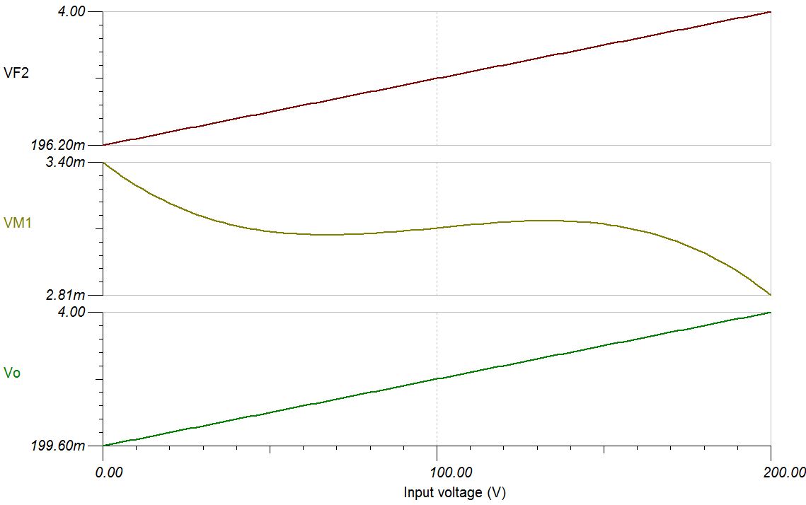
So when I change the circuit to my parameters, R1 = 2.49k, R2 = 25.45k, R3 = 45.55k, R4 = 1k,  R5 = 60.54k. I come up with this.

Here is the source

/cfs-file/__key/communityserver-discussions-components-files/14/6011.RTD_5F00_Linearization_5F00_Op_5F00_Amp_5F00_Circuit_5F00_Revised_5F00_Params.TSC

Are there any other recommendations that you would suggest implementing or revising with this circuit and using the TLV333?

Thanks

-David

  • Hi David,

    thanks for reaching out. It's good to hear that you tried to understand the simulation for the RTD linearization using different parts and it seems that you understood how it works.

    It is correct that the OPA333 has a smaller error at small low voltages due the offset voltage.  

    Consider that the voltage divider at R6 and R7 must not be populated on a pcb since it is for simulation measurements only.

    We can recommend using the OPA333 and TLV333 for the linearization at low voltages. The values from the excel sheet provide good values for a simulation and implementation.

    Regards,

    Miriam