This thread has been locked.
If you have a related question, please click the "Ask a related question" button in the top right corner. The newly created question will be automatically linked to this question.
Hi team,
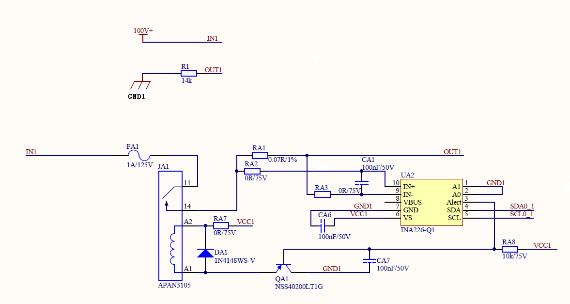
The customer is using INA226. The schematic is in the attachment. VBUS pin is not used and it is floating.
The load is the 14K resistance R1. Rshunt is RA1 and it is 0.07ohm. The current that is measured is 7.1mA.
JA1 is a relay. If the voltage is add to 11 pin and 14 pin, the internal switch of the relay will be closed.
For INA226, the Calibration Register value is 0x0725. The Mask/Enable Register value is 0x0003.
Case 1: 100V is connected to IN1 and OUT1 is connected to GND. The internal switch of the relay JA1 is closed.
Then the Shunt Voltage Register can be get the voltage and the voltage is 0.07ohm x 7.1mA = 0.497mV.
The Mask/Enable Register is 0x000B. The Calibration Register value is 0x0725. For case 1, it is fine.
Hi Mickey,
100V into the INA226, it is completely out of spec… but we might be able to find a workaround for that with a bit of thinking.
So, as far as I understand, no voltage readings are required, only current. So given you are doing a high side sensing, your customer requires a separate power supply to feed the INA226 with respect to IN1, that, I suppose, sits at said 100V. So, measured from GND, IN1 will be at 100V and the INA226 VCC will be 103.3V. The inputs of the INA226 will only see a low side common mode measurement with the voltage developed across RA1 rather than the 100V of the supply. Please let me know if this is clear or you need me to explain further.
The drawbacks:
We also have a reference design, that explains how to use an OPAMP to create a current source based on the voltage developed across the high side resistor. and hence shift the high side current measurement to a potential close to GND, so that the device can stay referenced to GND, thus not requiring an additional power supply or level shifting isolation, at the expense of some extra circuit complexity, power dissipation and board layout. You can find it here.
So it all depends on what your circuit requirements are (preference for cost, complexity or solution size), but I trust I provided a few ideas that will guide you on the right path.
As always, please feel free to left us know should you require further assistance.