This thread has been locked.

If you have a related question, please click the "Ask a related question" button in the top right corner. The newly created question will be automatically linked to this question.

OPA1611: Distortion vs load dependency

Part Number: OPA1611
Other Parts Discussed in Thread: OPA1612, OPA1622

We have a question for the OPA1611 amplifeir:
and the graph of Figure 7. THD+N Ratio vs Frequency.
It shows that amplifier distortions are higher for the load resistance of
600 Ohm than for 2 kOhm. Can you please explain what the reasons are for
this behaviour ? Is it e.g. due to the amplifier being forced to work with
bigger voltage difference at the inputs (to drive the amp properly to
provide the higher output current) ?.

In our case we need to handle low
resistance loads in the region of a few hundred Ohm. Is it a good idea in
order to achieve distortion reduction to use a simple wtórnik_emiterowy like
that (using a low-noise transistor and RE of 75 Ohm) ?
http://www.piclist.com/images/ca/ualberta/phys/www/http/~gingrich/phys395/notes/img630.gif

I would aprreciate an answer possibly soon as tho is the last missing bit to finalize our PCB design.

Regards, Pawel

  • Pawel,

    There are several reasons why for smaller RL, and thus higher output current, Iout, THD+Noise increases:

    For one, the overall AOL gain is composed of the gains of all the op amp stages including the output stage where the gain is defined as G=gm*Rout=(Rc||ro)/re=~RL/re; as RL gets smaller the gain of the last stage gets smaller resulting in lower overall AOL (see datasheet AOL for different RL).  Therefore, for lower RL, the overall loop-gain,−Aβ,  decreases for a given close-loop gain resulting in higher non-linearity.  

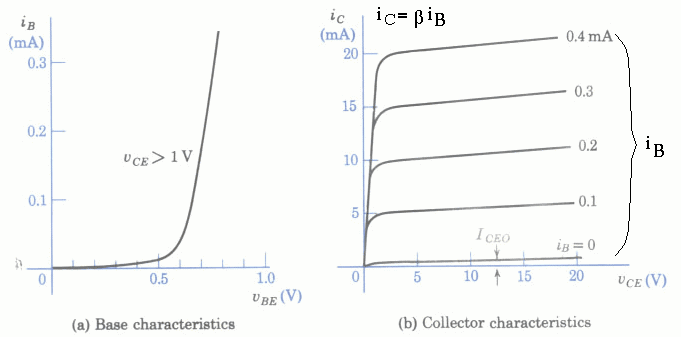
    Additionally, a higher output current, Iout, requires higher bias current, IB, to be delivered to the bases of the output transistors which forces the previous stage to work extra hard to meet the required bias current demend and this means higher non-linearity. Then you also have the effects of the collector parasitic resistance as well as increase in Vbe that causes the slope of IC vs Vce characteristics to be steeper (see below), which varies Ic with change of Vce (Vout).

    Wtornik emiterowy adds impedance at the emiter of bipolar device and thus will cause higher non-linearity and thus lower THD.

    Please take a look at OPA1622 - it will result in lower THD then OPA1612 under heavy loads.

  • Thanks Marek for the fast response. Excuse having forgotten to replace "wtornik emiterowy" with the English term although it was not a problem for you :)
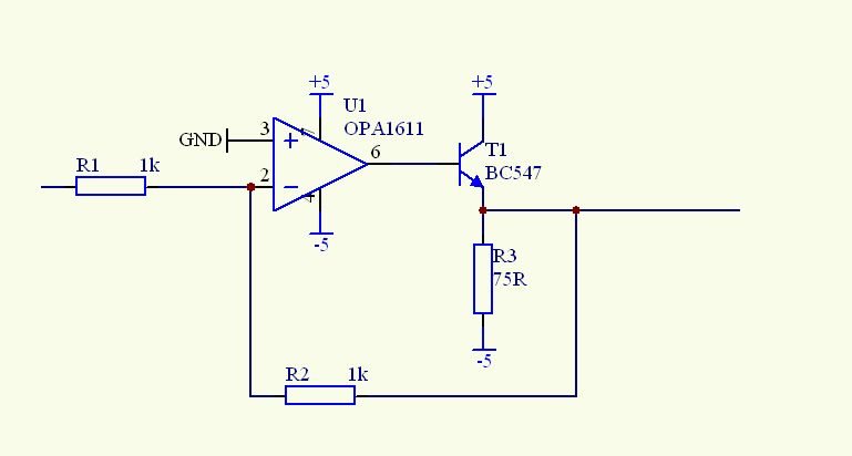
    Just to be more precise on the technical side with the emitter follower - we meant using it just on the amplifier outputs before the feedback loop not outside the feedback (and the feedback then taken from the emitter follower outputs) as shown in the picture attached. What is your opinion on using this circuit with OPA1611?

  • The external emitter follower circuit you show above will allow you to significantly increase the output current without much change in the output current of OPA1611 so you will improve THD performance but only at the base of T1 (pin 6 or Vo).  However, since the output signal, VOUT, is a voltage divider of Vo between re of T1 and R3, Vout=Vo*R3/(R3+re/), as you vary the output current in T1 you will modulate re=Vt/Ic=~(kT/q)/Ic, which will create the distortion you tried to eliminate.

    Therefore, the devil is in the detail whether the amount of improved distortion at Vo (due to lighter load) will or will not be offset by the higher distortion created between Vo and VOUT.  Thus, in order to answer your question, you will need to use specific transistor model of T1, gain, and specify the exact output current level to make such call.

  • It seems to us that the distortions you mentioned - as you vary the output current in T1 you will modulate re=Vt/Ic=~(kT/q)/Ic - should be eliminated by the feedback loop in the circuit. We think in this case the distortions should only be caused by the amp being unable to precisely follow and compensate the voltage error - would you agree ?
  • One more comment: in our design the emitter follower does not only work as a separate current amplifier to deal with the heavy load. In our case the emitter follower becomes part of the main amplifier and the feedback goes from the emitter follower outputs not the OPA1611 ones. So we want the feedback to compensate for the total distortions of both the OPA and the follower.
  • Pawel,

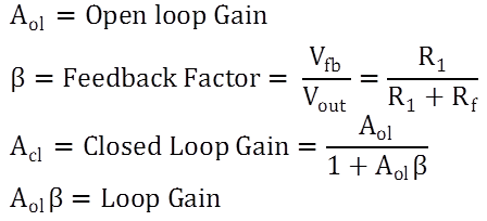
    Yes, I understand that in your circuit the feedback is closed from the emitter and not base of T1 but that only means that instead of seeing Vout=Vo*R3/(R3+re) you will have:Vout=Vo*R3/(R3+re/Aβ) where Aβ is a loop-gain - see below.  But since Aβ is NOT infinite, and it decreases over frequency as AOL roll-off at -20dB per decade, around -3dB point of close-loop gain (effective bandwidth) the amount of feedback benefit will amount only to a factor of √2.  Therefore, Vout(-3dB)=Vo*R3/(R3+re/√2).


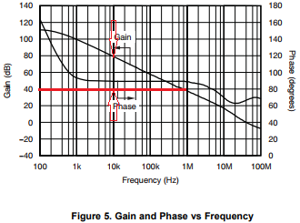
    Therefore, for the close-loop gain of 100 (40dB) and Iout of 100mA, at 10kHz frequency (see below) the distortion may be as high as:

    Distortion[%]=~(re/Aβ)/RE*100=~(0.25ohm/100)/75ohm*100%=~0.0033% where re=Vt/Ic=~25mV/100mA=0.25ohm and Aβ=80db-40dB=40dB (100 on linear scale).