This thread has been locked.

If you have a related question, please click the "Ask a related question" button in the top right corner. The newly created question will be automatically linked to this question.

Advise for precision, low-voltage input amp / circuit.

Other Parts Discussed in Thread: OPA197, TINA-TI, TLV3201, REF3225

This is my first post, thanks in advance any and all answers. 

I'm making 10 test units which need to be field proved. The design parameters are:

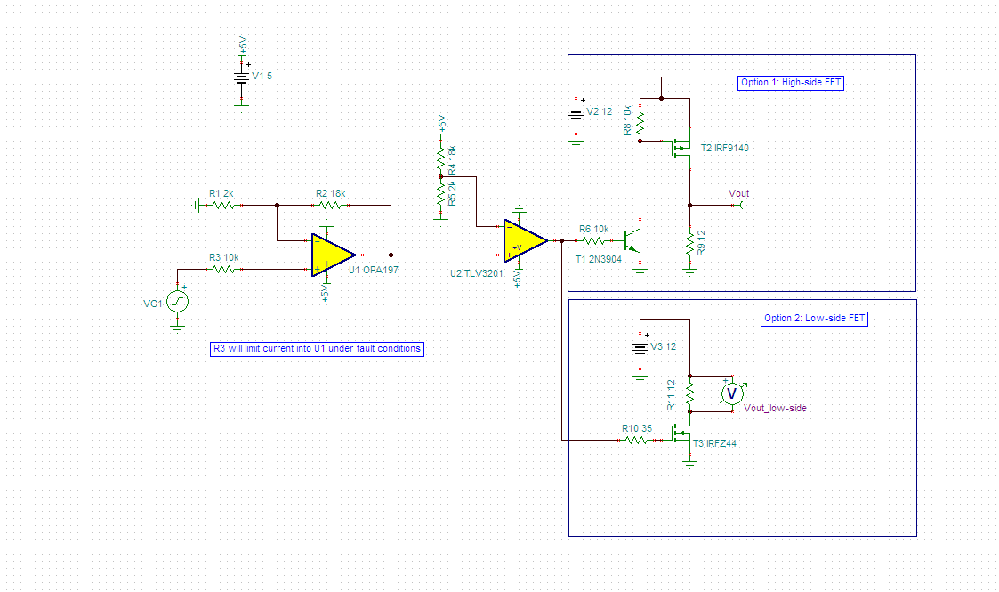
1) High input impedance (at least on par with a Fluke 87, or better) input measuring from 1 to 51 milli Volts DC--accurate to within 1 millivolt. (the range might ultimately be extended to 100 milli-Volts)

2) The above, at a set value (say, 50 milli Volts)  switches a D.C. inductive load up to approx. 1 Amp. (basically, one or more Bosch style relays, probably either resister or diode suppressed at the input coil) NOW.

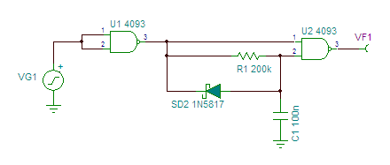
3) A timer/delay circuit involved in, or attached to, the above which can be adjusted from approx.  .5 to 3 seconds--this part so the above won't continuously cycle.

4) All the above mess powered from approx. 12-48 Volts D.C. of nasty vehicle power. 

5) Polarity protection to approx. 100 amps D.C. (this last part I was thinking of simply using a big diode, easy-peasy)

 I'm hoping for some industry-level, non-microprocessor prioritized chips as I want to avoid any reseting inevitabilities.

In the above, simplicity and robustness greatly trump cost. This circuit will be used in the vehicle industry, by less than careful hands. 

Thanks again for all input. 

  • Hi John,

    Here's what I'd recommend:

    Use an op amp configured as a noninverting buffer for your input. The TINA-TI simulation I'm attaching below uses an OPA197, which should give you at least 100MΩ of input impedance (for reference, the Fluke 87V has a 10MΩ input impedance). I configured this for a gain of 10, mostly so that errors further downstream (such as offset voltage of the comparator) should remain below the 1mV level you're looking for. 

    I followed the OPA197 with a TLV3201 comparator. The inverting reference to that comparator comes from a simple resistor divider, but could also come from a DAC or trimpot for easy reprogrammability. Whatever voltage is present at this input should equal your desired input trip voltage times your input amplifier gain.

    Note that the TLV3201's maximum supply is 5.5V. Since you're looking at low voltage inputs, I'd recommend using an LDO (and plenty of filtering) to drop your 12V vehicle supply down to a 5V supply for the amplifier, comparator, and other components. 

    I've also simulated the output stage. You really have two options here. Option 1 is a high-side drive, using a P-type power MOSFET. T1 and R6 level-shift the output of the TLV3201 to turn T2 on and off. R8 provides a pull-up to turn T2 off when T1 stops sinking current. Option 2 is simpler, using a single N-type power MOSFET to pull the low side of your relay coil to ground. 

    For both these options, I picked MOSFETs that were available in the TINA-TI libraries in order to get a working simulation. I'm not certain they're still available commercially, so substitutes may be necessary. For substitute parts, you'll need a power MOSFET that can support a continuous 2A (for a 2x safety margin) drain current for either the N or P type configuration. For the N-type case, you'll also need to ensure that the MOSFET's Vgs(th) is less than 5V, so that the TLV3201 (or other intermediate circuitry) can actually turn the MOSFET on.

    Keep in mind that at the full 1A load you mentioned, either of these options will dissipate around 1W of power. Heatsinking will likely be necessary for the power devices. The circuit as-drawn also does not protect the MOSFETs from being damaged by excessive current (a short, for example). It would be a good idea to add a fuse inline with the supply to this, if you weren't planning to already.

    One segment not included in the schematic above is the delay circuit. I think you have a couple of options here. If simple hysteresis (e.g. when the input goes above 50mV, the output turns on. When it drops below 48mV, it turns off) would work for your application, it's possible to add feedback to the comparator (U2) to make it behave as a Schmitt Trigger. Another option would be to add the circuit below between the comparator and output devices.


    For low-to-high transitions, this will behave like a buffer, and will pass the signal through immediately. For high-to-low transitions, C1 has to discharge through R1, adding a time delay. If the input returns high before that time has elapsed, C1 is discharged again, resetting the timer. By choosing appropriate values for C1 and R1, the delay time can be increased or decreased appropriately. Any small diode could be used in place of SD2, for example a BAT54 Schottky, or a 1N4148.

    One disadvantage with this circuit is that it has a fixed delay time before it will turn off. Even if the input drops dramatically below the setpoint, R1 and C1 still limit the response time. I think that for that reason, the Schmitt Trigger option is better - it gives you noise immunity near your setpoint, but will still react quickly to a falling input.

    EMI protection on this could be somewhat of a pain. Adding an LDO and properly filtering your supplies to the circuit should help cut down on noise leaking in through that path, but that still leaves the input and output as possible noise entrances. If you find that noise is coupling excessively into your input signal, I'd recommend adding a small amount of capacitance (say, 10nF or so) to the input, after R3. That should cut down on high-frequency noise coming into the input.

    Links: 

    TINA-TI schematic

  • Alexander, many thanks for your detailed solution. I need to go over this in the next week or two and if you don't mind, reply with comments/help for additional tweaks.

    Couple quick thoughts in the mean time.

    1) Delay timing isn't important as this delay is also being used as a form of indirect circuit protection--i.e., I want the monkey using this gizmo to know that when there is a problem, the gizmo will always react in the same manner (danger, Will Robinson!)--a circuit break from a fixed time delay should ultimately fix the appropriate user response.

    I'll probably add a buzzer and a big red led when the circuit trips.

    Thanks for the additional information though, as it's feeds my native "tweakyness".

    2) Perhaps more detail on the filtering issue; EMI is always a pain!

    Ingenious use of the dual nand gate with the "timer" in between one of the input legs of the second gate--I don't think I've seen that circuit since school--never would have quickly thought of that. That's why I'm here--good job. 


    Anyhow, more later, if you are game.

    Once again, thanks a bunch.

  • Hi John,

    There are a lot of good resources for EMI mitigation. For a more in-depth look at it, I'd recommend Henry Ott's Electromagnetic Compatibility Engineering. We also have some presentations about typical effects of EMI on precision circuits (such as this one by my colleague Thomas Kuehl).

    As a general rule, follow best practices for layout. Use a ground plane (if possible), keep loops small, keep decoupling and filtering capacitors close to active devices, and minimize the length of any high-impedance traces (the inverting input to the op amp, for instance). Doing this should help minimize the severity of EMI coupling indirectly into your system.

    Next, keep in mind that there are three possible conducted routes for EMI to get into your system: inputs, outputs, and power supplies. Inputs should be fairly easy to filter. The 10kΩ protection resistor on the op amp will give you some low-pass filtering for free, and if you need to you can always add additional capacitance to lower its cutoff. Using shielded cabling between the signal source and the circuit's input will also cut down on interference coupling to the input to begin with.

    For power supplies, adding ferrite beads and capacitors where the supplies come onto the board will help. Adding an LDO with additional filtering after it will add another layer of protection.

    Outputs may be trickier to protect. Adding capacitance to the output of an op amp to attempt to bypass RF energy to ground can cause instability even with relatively small capacitors. For the comparator in this case, stability shouldn't be a concern, and it should be possible to add capacitance to the output, but I'd recommend adding a small series resistance between the comparator output and the capacitor to decrease the peak current. Since this will behave as a low pass filter, it may slow down the turn-on of the output FET, increasing its power dissipation. In this case, it may be better to place a capacitor between the high-current output and ground. 

    I'd argue that for your circuit, the biggest worry would be noise at the input (or coupling into the op amp). The gain of 10 from that amplifier buys you more headroom in terms of SNR at the comparator, even if noise couples in. At the input amplifier, though, large spikes could quickly exceed your 1mV resolution. From that perspective, power supply filtering and input filtering (plus layout) will likely be the most important.

    Regarding the NAND circuit, it's something I came up with a while back to solve another similar problem. It is a pretty handy circuit to get a fixed (but asymmetrical) delay from an input signal. The only catch is that it requires a gate with Schmitt-trigger inputs like the 4093 to work properly. 

    One final thought: If this is intended to be a circuit breaker, it may be a good idea to invert the behavior of the circuit (this should be as simple as switching the two inputs to the comparator and the relay NO/NC terminals). In this case, if a fault is detected, or the circuit breaker loses power, downstream devices will be disconnected - it's fail-safe. With the circuit as-drawn, a power loss or failed component would prevent the output from turning off (or alerting the user), which could end badly unless there's a fuse or something downstream to cut the power in the event of a catastrophic fault.

  • Alexander,

    Yes, it's a circuit breaker.  As for the fail safe relay wiring, I will follow your advice and furthermore, hook up a buzzer and a big led to the NC connection. 

    "It is a pretty handy circuit to get a fixed (but asymmetrical) delay from an input signal."

    It's right up my alley as the delay occurs at the high-to-low transition; the asymmetry works perfectly to my advantage as I want this thing to time-out at the voltage decay--that is the tripping point where the error will occur so a moment's pause here is just perfect.  

    "I'd argue that for your circuit, the biggest worry would be noise at the input (or coupling into the op amp). The gain of 10 from that amplifier buys you more headroom in terms of SNR at the comparator, even if noise couples in. At the input amplifier, though, large spikes could quickly exceed your 1mV resolution. From that perspective, power supply filtering and input filtering (plus layout) will likely be the most important."

    My thought's too. Now, while I'll follow best practices, and maybe "cage" this thing in an interior metal box, I'm still very concerned with the chip supply for two reasons:

    1) Circuit stability (non-EMI issues) 

    2) Providing a constant, stable voltage source for the voltage divider at the comparator. As the latter provides the set-point for the circuit trip, and I'm working with tight specs (your 2 millivolt  leeway is about just right for this circuit), I need stability.

    I looked into LDO's but I haven't found anything which doesn't need added components. Do y'all offer any prefab circuits which I can buy?

    Yes, I'd rather buy than engineer. By the way, this is one of my first forays into a low magnitude analog (excepting your elegant gate timer) measuring circuit. I'm usually doing other stuff. 

    Thanks, and no need to answer right away; I greatly appreciate your input thus far. 

  • Hi John,
    I'd probably recommend something simple like the uA7805. It should really only require a capacitor on its input and output, and should give you a reasonably stable 5V output over temperature and input supply.

    As drawn, for a 50mV trip point, your input trip voltage will swing 1mV for every 100mV of supply shift. The uA7805 can shift around 100mV over supplies, and closer to 250mV over temperature. If higher precision is needed, you might consider using a precision reference such as the LM4128-2.5 or REF3225 powered from the main LDO. That would give you a much more accurate 2.5V reference which should hold constant over supply and temperature.

    In terms of power supply EMI, I think this leaves you in good shape. Any incoming interference will be attenuated by decoupling capacitors, then by the LDO's PSRR/Ripple rejection, then again by the PSRR of the op amp. On the reference signal, you have the advantage that the divider gives you a ~40dB boost to PSRR, and you could probably improve that by adding a decoupling cap to the reference.
  • Alexander,

    Thanks for the specifics; this clears up a great many interlocking questions. 

    Basically, thanks for building most of the circuit and detailing pitfalls.