This thread has been locked.

If you have a related question, please click the "Ask a related question" button in the top right corner. The newly created question will be automatically linked to this question.

INA139: ina139

Part Number: INA139
Other Parts Discussed in Thread: INA240

I have two questions about INA139. The first one is : Can i use the INA139 with a differential input voltage range from 100mv and 1.5V? How does it operate in this situation?

 .

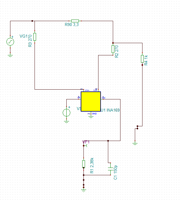
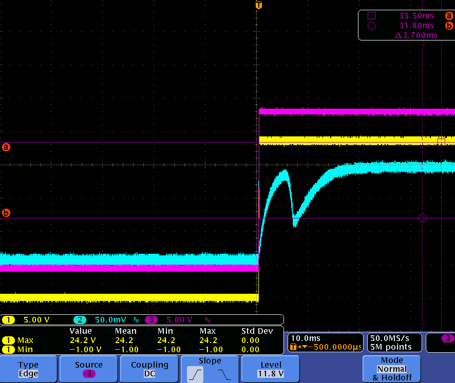
The second one is related to my design that doesn't work (figure above). I test the circuit in a real pcb situation. The input is a 24V ramp with 100us of trise. At the output, i have a delayed signal while the input is OK. Why do i have this behaviour? (figure below) output is the blue one, the other two are the differential input:

Thank you very much.

Regards

  • Hello Robert,

    For your first question, you can operate the part with a differential input voltage (Vdiff) range of 100mV to 1.5V since it is within the 2V Absolute Maximum Vdiff of the part, but you will have to ensure that voltage output is within the compliance range by selecting the correct RL and and power supply. Your maximum Vout will be limited by the lower of the following two equations from the datasheet.

    Once you calculate this, then you can calculate what your Iout will be for a Vdiff of 1.5V and thus what voltage should occur across RL. If RL = 2.38k and Vdiff = 1.5V, then Vout should be 1000uA/V * 1.5V * 2.38kOhms = 3.57V. You will want to make sure that the previous equations will allow this output.

    I'll note that the 270Ohm resistors into your input will decrease your DC accuracy due to the mismatch of input bias currents (Ib+ and Ib-) creating mismatches in voltage drops across them. We usually recommend keeping these resistors to 10Ohms if you are trying to implement a differential input filter with a differential cap. This is not explained in the INA139 datasheet but is explained in the INA240 datashet, section 9.1.1.

    For your second question, this behavior is due to the fact that you are operating the part outside of it input common-mode voltage range (2.7V < Vcm < 40V). You are not operating outside of the absolute max Vcm spec (-0.3V < Vcm < 60V) so this will not break the part.

    Peter Iliya

    Current Sense Applications

  • Hi Peter, thank you for the answers. For my first question, tha datasheet recomends a full scale input differential range maximum of 500mV; so I would like to know  how the part behaviour changes when I overcome this threshold ( es. from 500mV to 1.5V).

    For the second question, the two 270 ohm resistor represents for me the two channel ON resistance of a MUX that I have to use for switching the differential signals (for my application) ; so I can't neglet or eliminate them. 

    I don't understand why I am outside the input common mode voltage, as you said. My input common mode voltage(as you can see from the figure) is maximum 24V.

    If in the future I will have non a load resistor but an inductor whose I would like to monitor the current , will the part work properly?

    Thank you a lor, regards.

  • Hi Peter, thank you for the answers. For my first question, tha datasheet recomends a full scale input differential range maximum of 500mV; so I would like to know how the part behaviour changes when I overcome this threshold ( es. from 500mV to 1.5V).

    For the second question, the two 270 ohm resistor represents for me the two channel ON resistance of a MUX that I have to use for switching the differential signals (for my application) ; so I can't neglet or eliminate them.

    I don't understand why I am outside the input common mode voltage, as you said. My input common mode voltage(as you can see from the figure) is maximum 24V.

    If in the future I will have non a load resistor but an inductor whose I would like to monitor the current , will the part work properly?


    Thank you a lot, regards.
  • Robert,

    I am still looking into how the behavior changes when your Vdiff passes 500mV. For the time being you are operating the part outside of its Vcm range because the Vin+ is at 0V before the 24V step input. If your step started a 2.7V and then ramped up to 24V, then your part will be operating inside its Vcm range the entire time.

    Peter Iliya
    Current Sense Applications
  • Hi, thank you for the answer. Ok, I understand that during the ramp for few microseconds i am outside the input common mode range. But being in this situation could bring the output voltage to assume that behaviour(so show a delay of 20ms)or it is due to other phenomena?
    Thank you again.
  • Robert,

    To answer one of your earlier questions, the reason we reccommend (for the most accurate measurements) that INA139 Vsense be limited to a full-scale range of 100mV to 500mV is because this is the range you will get the best DC accuracy and gain drift from the current output of the part. Additionally, this is the range chosen as the test conditions for most of the electrical characteristic specifications in the datasheet. This means that if you are within this sense voltage range (100mV to 500mV), you can be most confident that your device will adhere to these specs since this is what we will guarantee.

    The technical reasoning is that the output stage current source has a limited internal gain which can be trimmed initially, but will begin to change for Vsense > 500mV and vary with temperature. This will contribute to gain drift over temperature.

    -------

    Anyway, I see that you are seeing this "20ms delayed" output when driving a solenoid here as this E2e thread:
    e2e.ti.com/.../634684

    Please provide a scope shot of the actual differential voltage either by using a differential probe or using the post-processing math feature of your scope so we can see the differential voltage and Vout during this 24V ramp.

    Peter Iliya
    Current Sense Applications
  • Hi,thank you for all. I discovered that the output profile is due to the input differential voltage applied to INA and not due to a component limitation.

    Last question: If I use a full scale range of 500mV, how much is the resolution, so I mean the minimum differential voltage I can apply to the INA, in order to see at the output a correct voltage ?

  • Good to hear Robert.

    This is not really something we specify and how to define a correct voltage (define the error) will change this answer. There are some things that can be said:

    1. If your Vsense is in between 10mV and 150mV, you can expect the part to output a current with a transconductance of 990uA/V to 1010uA/V. You can also expect the non-linearity error to be +-0.13% maximum (+-0.01% typical).

    2. According Figure 4, your total ouput errorto be around -13% at 25C for a Vsense of approximately 7mV. We do not have data for smaller Vsense voltages.

    Best,
    Peter Iliya
    Current Sense Applications
  • Hi Peter, I understand it.

    I am following a design with INA139. A part from the problem I solve thank to your support, I have another question I don't understand in the datasheet of the component pag.9 eq1 and 2. If I supply the INA139 with 5V and I have a differential input voltage of 1V into a sense resistor of 10ohm with a INA139 resistor load of 3kohm, I will have about 3V at the output and a maximum output voltage swing of 3.3V? But If i increment the differential voltage to 1.3V how much is my output voltage? will it be the saturation voltage (5-0,7-1.3=3V)? if it is so, I will not able to recognize if the 3V comes from a differential voltage of 1V or 1.3V? Correct?

    Thank you, regards.

  • Hey Robert,

    What you have described is correct. The output compliance voltage of the INA139 is always limited by the shunt voltage (Vdiff), input common-mode (Vcm = Vin+) and power-supply (V+). If you need more compliance voltage headroom you could power INA139 with the bus voltage rail of 24V.

    Peter Iliya
    Current Sense Amplifiers