Because of the Thanksgiving holiday in the U.S., TI E2E™ design support forum responses may be delayed from November 25 through December 2. Thank you for your patience.

This thread has been locked.

If you have a related question, please click the "Ask a related question" button in the top right corner. The newly created question will be automatically linked to this question.

INA180: Protecting the device against Transients Greater Than 26 V

Part Number: INA180
Other Parts Discussed in Thread: TIDA-00302,

Dear All ,

I am working on a Current sense application of and control circuit for a solenoid valve in an Automotive application ,The Control Circuit has a Free wheeling Diode and snubber circuit in parallel to the solenoid coil.

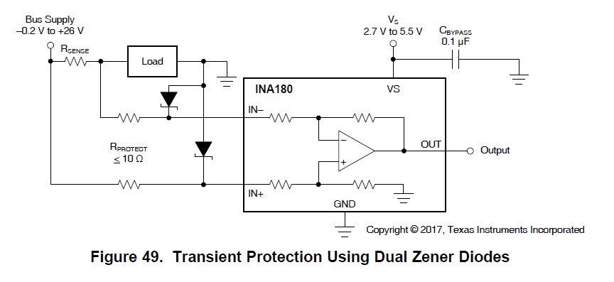
From the data sheet( page 25) I would like to implement the circuit as shown in attached picture and would like to ask a few questions with the hope of some advice or guidence

(1) from simulation of the Solenoid and Freewheeling diode I can expect a Inductive voltage spike of around 16-18V (with out Free wheeling Diode it is above 30V ,what should I use for the protection zener diodes D2/D3

I think 18V ?

(2) Is my implementation of the Diodes correctly place and connected the datasheet recommend resistor values smaller than 10 Ohm will 4.7 Ohm be OK ?

EDIT: I also would like to know if there is a specific Zener diode series to be used (which has the correct reaction Times) or would any standard Zener series work such as the BZX55C(500mW) ? 

Thank you very much for any guidance it is highly appreciated

  • Peter,
    Due to the holiday, our responses will be delayed. In the mean time, take a look at TIDA-00302 to see how to protect against transients in general for current shunt monitors. We'll review your questions more in the next couple days and get back to you.
  • Jason.

    I understand perfectly it is holiday time no problem at all,Thank you for the link it seems my thinking is in the correct direction, However the main issue for me is the actual values of the zeners and Resistors ,

    Happy Holidays
  • Hi Jason.

    I have read through the TIDA reference design and also searched the TI Application notes and all seems to show / explaining the protection referenced as a High side  current measurement.

    This is exactly where my problem is I am not sure what the effects of the transients  is in  a low side current measurement and load dump and how should the INA180 be protected in a low side configuration,The basics around the High-side is clear from the Reference design and  how to apply it to a design but as said not really anything on the low side configuration it is either one of the following

    (1) it has no influence on the device

    (2) you can apply the exact same protection as for the high side 

    Also in the data  sheet the reference is to High side 

    I appreciate any help or direction here as I am not a very experienced Analog designer 

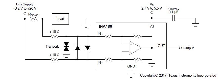
    From the TIDA Reference design

     From the Data sheet

  • Peter,
    If you're concerned with transients caused by things like ESD zaps, then the same protections should apply regardless of high or low side configurations as those can be hundreds to thousands of volts in a spike. Now, if you're worried about something like a few volts of overshoot from a 0V to 24V common mode (where you could spike up above 26V) then those are less applicable with low side configurations because your common mode always sits around 0. You could still have overshoots below ground around fast edges, which you should be careful with because the inputs should stay above -0.2V (for the ina180, other parts are different. This is where the parts are specified and the ESD cells can start to activate if you go too low.)
  • Hi Jason,

    Thank you for your reply and good advice ,

    If I understand you correctly basically I can implement the protection circuits connections as shown by the reference design and the try to find/ calculate correct values for the zener diodes or Tranzorb Diodes.

    From the reference design it seams that the Tranzorb diodes was not very effective and the use of the zeners did better protection.

    so this leads me to Ti what would you recommend as a basic circuit for our low side measurement with the INA  as clearly I am more concerned of the spikes from the Inductive coil than ESD 

  • Hello Peter,


    Jason asked me to work with you in case you have further questions.


    Theoretically the Drain terminal of the NMOS experiences a PWM signal of 0V to ~12.5V. In reality depending on how well the PCB is made, there will be overshoots. Maybe this is where you see the 18V?


    The Source terminal should stay at ground level at all times. As Jason pointed out, the configuration is low side sensing, the common mode that INA180 sees is zero volts, it should never be 18V. The protection diodes are really not necessary in my opinion.


    But I look forward to your further comments.


    Regard, Guang

    Apps Support-Current Sensing

  • Hello Guang.

    Thank you very much for your reply and valuable information.

    I came to the same conclusion as you and Jason and I appreciate all the time and effort you have taken to discuss this with me and the confirmation I have now makes me feel more confident to proceed with the design .

    Just another question I think I would place the Low pass filter in front of the INA  would you recommend the use of the LPF ,

    Again thank you very much 

  • Hello Peter,


    Yes a filter, as outlined in section 9.1.3 in the datasheet, is optional and can be employed for for improved signal quality. In general we recommend such filter since it doesn’t take up much space/cost.  


    Regard, Guang

  • Hi Guang ,

    Thank you for your info and confirmation,I am a LPF freek ,I like to use them all over  :)

    Have good time