This thread has been locked.

If you have a related question, please click the "Ask a related question" button in the top right corner. The newly created question will be automatically linked to this question.

Stability of Differential op.amp with Gain<1V/V (THS4521)

Other Parts Discussed in Thread: THS4521, TINA-TI

Hi all,

I have a beginner question, but somehow I have internal disagreement in that aspect.

I'm have design of system with diff op amp THS4521 that Gain is lower than 1

(Gain<1,   Gain =Rf/Rg=Vout/Vin=0.1)

1.       Please advice how can I test the stability of this circuit in spice simulator (i.e. Gain x Phase (in open loop?))?


1.        If I'm know that the degree of an amplifier's stability can be quantified by a so-called stability factor


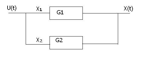
and the system will be stable at G1xG2 /= -1

In my case the G1< 1, so it means that system always are stable???  Please advice if I'm wrong.

I sow in some datasheet that written the "Amplifier is stable at Gain=1V/V".  So what happen if Gain <1V/V ?

 Thanks a lot for help. Roman.I.


TH4521_ETE_TI_Question01.docx
  • Normal 0 false false false MicrosoftInternetExplorer4

    Hi Roman,


    For regular op amps, the minimum gain stability is given for the non-inverting or noise gain configuration, i.e. for inverting gain of -1, the non-inverting gain is +2V/V. That means that for unity gain stable op amps, it is possible to configure them with Rf < Rg for inverting attenuation because the overall noise gain is still greater than unity gain.


    It is a little confusing for fully differential amplifiers because an FDA can be seen as two inverting amplifiers in a parallel differential architecture. Op amp stability is concerned with the noise gain, however, and the noise gain of an FDA is still the same as for a regular op amp, 1+Rf/Rg. That is, an FDA in a differential gain of 1V/V (Rf=Rg) will have a noise gain of 2V/V. FDAs are typically internally compensated for stability at noise gain of 2V/V, or 1V/V differential gain.


    The best way to test out if an attenuator configuration will work is on the bench, however, it is possible to simulate the loop gain and measure the phase margin. But I must warn you, the THS4521 Spice Model macro code mentions that the open loop gain response is not accurately modeled. Still, the simulation should serve as a good approximation of what to expect on the bench and will get you in the ballpark of what noise gain compensation to use.


    The G1*G2 you mentioned, or loop gain, for a fully differential amplifier can be simulated by injecting a signal into the feedback loop. Below is the circuit I used to simulate the loop gain of your circuit:


    Normal 0 false false false MicrosoftInternetExplorer4

    As you can see, I’ve terminated the gain setting resistors to ground and used a couple of ideal voltage-controlled voltage sources and a couple of large capacitors and inductors to inject a differential signal into the feedback loops. The large 1TF caps and large 1TH inductors ensure that the DC operating point of the amplifier is preserved, at the same time allowing the small injected signal into the amplifier + and – inputs to be measured around the loop at the LoopGain probe. An AC sweep will return the Loop Gain and Open Loop Gain (Aol) of the amplifier circuit. The results of my simulation are below. The burgundy trace is the amplifier’s open loop gain, Aol, whereas the green trace is for the loop gain. Measuring the phase margin at the loop gain’s 0dB crossover point shows that the phase margin is 73.46°.


    Normal 0 false false false MicrosoftInternetExplorer4

    I attach a zip file with my TINA simulation circuit file, and the images above (I'm guessing they're not showing up very well). The same injection method should work in Pspice. A free version of TINA is available here: http://focus.ti.com/docs/toolsw/folders/print/tina-ti.html


    Also, here are a few links to a series of app notes on the topic of using fully differential amplifiers as attenuators:

    -          Using fully differential amplifiers as attenuators – Part 1 – Differential bipolar input – http://focus.ti.com/analog/docs/litabsmultiplefilelist.tsp?literatureNumber=slyt336&docCategoryId=1&familyId=1453

    -          Using fully differential amplifiers as attenuators – Part 2 – Single-ended bipolar input – http://focus.ti.com/analog/docs/litabsmultiplefilelist.tsp?literatureNumber=slyt341&docCategoryId=1&familyId=1453

    -          Using fully differential amplifiers as attenuators – Part 3 – Single ended unipolar input – http://focus.ti.com/analog/docs/litabsmultiplefilelist.tsp?literatureNumber=slyt359&docCategoryId=1&familyId=1453

    THS4521 Loop Gain.zip
  • Good morning Kristoffer,

    Thanks for great explanation and cleverer method of injection signal into the feedback loop.

    It's my first time using TINA, very friendly spice application. 

    If u have some time pls. see updated simulation of LoopGain in TINA vs. Pspice in doc attached.

    If I understand u correct the LoopGain is G1xG2=βAOL, when Aol is a G1 (according to block diagram above).   

    1.       Can you also suggest circuit for single ended LoopGain simulation? (injection of signal into the feedback loop of VFB) 

    2.       Do u have an idea where I can find VCVS component in Cadence PSpice and in TINA? 


    3.      Sorry but I'm still a little bit confused, dose LoopGain=G1*G2= βAOL .

    * As I understand, the LoopGain@0db must have Phase <(180°-45°), so in my case the circuit doesn’t in unstable boundary limits. (I got OpenLoop phase margin is ~57.66°<135°).


    TH4521_ETE_TI_Question02_1.docx
  • Hi Roman,

    I cannot take credit for coming up with the injection circuit. It is a method I learned from the gurus here at TI :)

    1) The loop gain can be simulated for a regular op amp using the configuration below:

    2) The VCVS should be under the Analog parts library in PSpice. I believe the part is labeled as 'E.' Unfortunately, the VCVS in the free version of TINA-TI is not available in the menus, however, you can copy-and-paste the part from my simulation into your own schematics.

    3) The loop gain is the gain around the feedback loop, which includes both the forward gain Aol  and feedback factor β, so the loop gain is Aol*β. For stability, the phase margin should be >45° where the loop gain magnitude crosses 0dB.

    One precaution about using these loop gain simulations is that the results are only as accurate as the op amp models being used. The op amp open loop gain and output impedance must be modeled accurately especially for simulations of op amps driving capacitive loads.

    Here is a link to TI-contributed article series on op amp stability that may be of interest to you:
    http://www.en-genius.net/site/zones/acquisitionZONE/technical_notes/acqt_092407

  • Kristoffer hi,

    Thanks a lot for reply, now the op.amp stability issue is clear to me J

    Have a good day,