This thread has been locked.
If you have a related question, please click the "Ask a related question" button in the top right corner. The newly created question will be automatically linked to this question.
Hi
I want make pcb for below schematic..in this schematic PWM DRIVE Q1 SO L1 draw 3A .U1 (OP AMP) INVERTING INPUT FEED FROM R3..
BECAUSE L1 CONSUME HIGH CURRENT I WANT SEPARATE L1 GROUND PLANE FROM PRECISION CIRCUITS GROUND PLANE .
BUT MY QUESTION IS : HOW CONNECT R3 TO U1 (OP AMP PIN 2) OVER GROUND PLANE GAP?? IN WHOLE PCB TIPS RECOMMENDED NOT PASS TRACE OVER GROUND PLANE GAP !! ON THE OTHER HAND RECOMMENDED PARTITIONING GROUND PLANE FOR NOISE IMMUNITY .
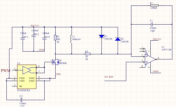
I DRAW A LAYOUT AND PUT HERE FOR SAMPLE .
IN THIS PCB LAYOUT I CONNECT TOW GND PLANE WITH A BRIDGE AND CONNECT R3 TO U1 OVER THIS BRIDGE.
THIS MANNER IS TRUE??
THANKS.
SINCERELY .
Hi Reza,
it's always a good idea to think about how the currents flow, which currents are noisy and which currents are vulnerable to noise. First, there is U2, Q1 and C5. Their currents are fast and noisy. These parts profit from the ground plane! Turn C5 a bit and move it so that it is on top of U2 package. By this you decrase the distance between its ground pin and the ground pins of U2 and Q1. And don't connect pin 1 and pin 8 of U2 in the ground plane. Between output of U2 and gate of Q1 I would insert a small resistance. This can reduce gate current spikes.
Then there is this huge current through L1. Think about how this current is flowing: Out of C2, C3, C4, through L1, through the ground pin of Q1 and back to the ground pins of C2, C3, C4. With the arrangement of C2, C3, C4 of your PCB layout you force this current to flow across the whole PCB. This is not good. Move the caps down, under Q1, and locate these caps in such a way, that all their ground pins have closest distance to another and to the ground pin of Q1. Now, connect these ground pins together with short and fat traces. Yes, now these ground currents no longer flow within the ground plane but have separate copper traces. Make a connection to the ground plane only at the ground pin of Q1.
Now you can remove the gap in the ground plane at U1.
Another hint: Do never route traces in the ground plane. Use bridges for that or use a multilayer board. A ground plane must be solid and massive. Only then the ground plane has extremely low inductance.
Kai
Hello Reza,
I tend to agree with Kai that with good component placement and wide traces for high current GND paths back to Q1 GND, that a single ground plane can work best. I think Kai meant to say don't connect pins 4,5 of U2 to the ground plane though (pins 1,8 are VDD). The techniques described are similar to what we advocate for many of our power controllers. See http://www.ti.com/lit/ds/symlink/tps40200-q1.pdf layout guidelines for example. Another idea you might want to consider is to remove the GND plane under the traces that connect U1 input to the input resistor and its feedback resistor. That way you've minimized trace to GND plane capacitance that could couple high frequency noise from GND into the high impedance op-amp input.
Dear Jeff,
yes, pin1 and pin8 of U2 should both be connected to Vdd. But in my computer screen it looks like Raza has made this connection with a blue copper trace, or by other words a copper trace which is routed in the same plane as the ground plane. I meant he shall make this connection not in this plane (the ground plane) but in the plane which has the copper traces red. This in order to keep the ground plane solid. The ground pins 4 and 5 of U2 should be connected to the ground plane, like Raza has already done.
In our experience very high currents like those flowing through L1 should not run in the common ground plane, because they can shift the ground potential within the ground plane and introduce common mode noise. This can make the PCB "radiate" in the CE testing.
Kai
Hi
THANK FOR ANSWERING .
I CORRECT PCB AND REDRAW .MY QUESTION IS ABOUT COMPONENT PLACEMENT AND GROUND PARTITIONING .
I REDRAW GND OF C2,C3,C4 ACCORDING TO YOUR GUIDE.
BUT MY SCHEME HAVE MORE COMPONENTS AND PUT BELOW LAYOUT.(TWO LAYER)
PLEASE GUIDE ABOUT BEST COMPONENTS PLACEMENT AND GND PARTITIONING DUE TO THE U5=ADS8329 16BIT ADC AND U6= UC.
(COMMENT:WHEN U5 WORKING AND SAMPLING Q1 IS OFF)
THANKS
SINCERELY
Hello Reza,
It looks like you removed a small portion of GND plane at the input to U1. If the intent is to reduce capacitive coupling of noise from GND at the input you would have to clear the GND plane for 5 - 10 mils on either side of the input trace back to the input resistor, diodes and amp feedback resistor. However, since the high power portion of the layout has been cleaned up, this is probably not necessary. I also feel that you do not need the GND gaps on the right side of the board.
If you need more guidance on the A/D portion of the layout, please post a new thread in the Precision Converters Forum and the A/D experts for that device can help out.
Hi
THANKS FOR ANSWERING.
I REDRAW LAYOUT AND PUT AGAIN.I DO Kai RECOMMENDED ABOUT L1,R2.
I CONNECT NEGATIVE PIN OF C2,C3,C4 TOGETHER SO CONNECT TO Q1 GROUND PIN.UNDER THIS TRACE CUT GND PLANE FOR REDUCE STRAY CAPACITANCE .
I DO NOT INSERT LDO AND VOLTAGE REFERENCE CHIP AND U6 CONNECTIONS ON SCHEMA FOR SIMPLICITY .I PUT STATEMENTS :10V REF AND 5V REF AND OTHER FOR SIMPLICITY.
U5 IS A 16BIT ADC AND CONTROLLED WITH U6 UC . I PARTITIONING GROUND PLANE UNDER U5 FOR SEPARATE ANALOG GROUND FROM DIGITAL GROUND.(AND PUT DECOUPLING CAPACITANCE
FOR U6 UC POWER PINS IN DIGITAL AREA).
IN WHOLE PCB LAYOUT DOCUMENTS RECOMMENDED NOT DRAW TRACE OVER GAP OF GROUND PLANE BUT JEFF RECOMMENDED CUTOUT GND PLANE UNDER INPUT TRACE TO U1 FOR
REDUCE STRAY CAPACITANCE . WHAT IS YOUR RECOMMENDED ABOUT TRACE OVER PLANE CUTOUT ??
I DRAW POWER SUPPLY TRACE FOR U1,U3 UNDER R3,D1,D2.THIS MANNER IS TRUE OR FALSE .
I DRAW POWER TRACE FOR U6 AND DIGITAL SEGMENT OVER AREA HAVE NOT GND PLANE UNDER TRACE .THIS MANNER IS TRUE OR FALSE .CAN I PUT POWER SUPPLY TRACE ON AREA HAVE NOT GROUND PLANE.!
SINCERELY