This thread has been locked.

If you have a related question, please click the "Ask a related question" button in the top right corner. The newly created question will be automatically linked to this question.

OPA192: OPA192 input protection w.r.t. input current and Vcm

Part Number: OPA192


Hi team,

I have tired making sure how we could implement the input protection for OPA192 with input current limit resistor.
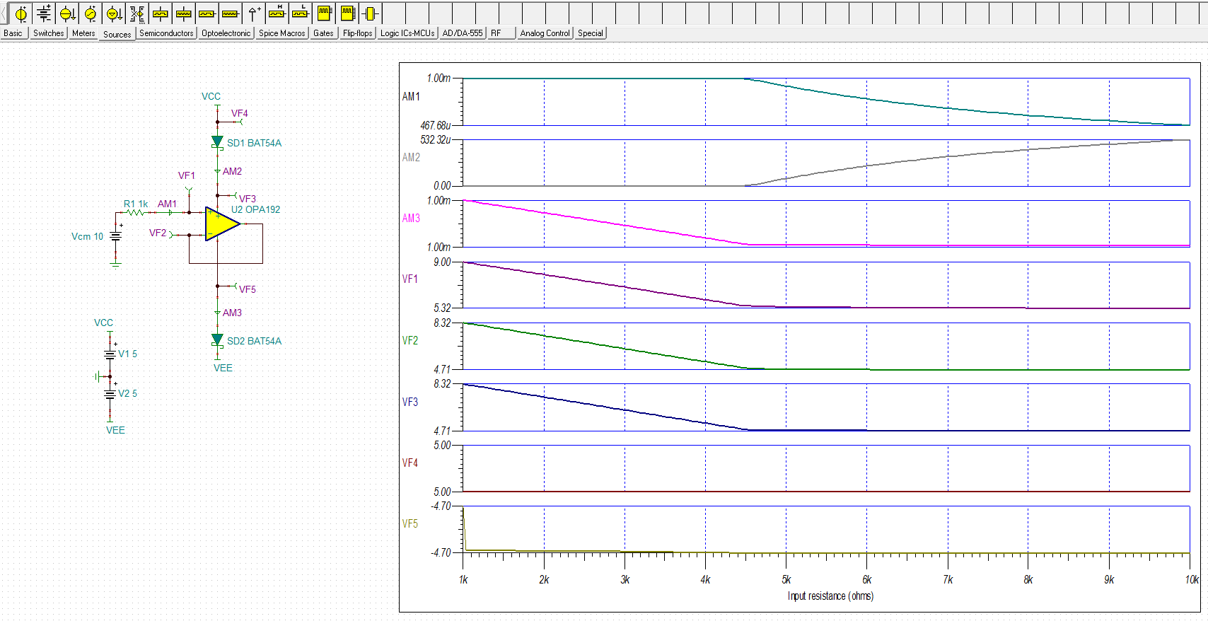
As you can see in the attached simulation, even if input current is limited within 10mA, Vcm could violate the ABS...

OPA192_protection03.TSC

In the case of actual circuit, should we maintain Vcm ABS when designing the input protection?

Best regards,
Iwata Etsuji

  • Iwatsu-san,

    There is an issue with your OPA192 TINA simulation circuit that is leading to erroneous conclusion. The voltage source, or batteries, in the circuit are ideal. They have zero impedance and can both sink and source current. For those reasons the results produced are likely quite different than what would be obtained using real and practical voltage sources such as voltage regulators.

    Voltage regulator ICs can sink or source current, but not do both. Therefore, if the supplies are made to perform that way in the simulation, the results will different than what you originally obtained.

    The voltage sources in the simulation circuit can be altered by adding a diode in series with them making them unidirectional. You can see this in the circuit shown here:

    OPA192_VCM_ESD_01.TSC

    When the current is blocked from flowing into the Vcc source, the input current is limited to 1 mA by the 1 k ohm series input resistor. VF3 rises to about 8.3 V, but that is safe for the OPA192. Note that no current flows into Vcc.

    Regarding your question: In the case of actual circuit, should we maintain Vcm ABS when designing the input protection?

    If the OPA192 Vcm is driven beyond its linear range it doesn't damage the op amp providing the Absolute Maximum Ratings voltage and current aren't exceed in some way. Choosing a sufficiently high value series input resistor that limits current to less than 10 mA will assure that the OPA192 won't be damaged.

    Regards, Thomas

    Precision Amplifiers Applications Engineering

  • Iwata-san,

    Did this answer your OPA192 inquiry? If so, please close the thread. If not, let us know how we can help.

    Regards, Thomas
    Precision Amplifiers Applications Engineering
  • Hello Kuehl-san,

    Thank you for your support.

    I believe reply should be the answer.
    However, we would like to make sure another simulation I had done.

    OPA192_protection01.TSC

    I expected the attached should clarify how Vs source circuit could have any influence.
    Do you think the attached is also improper? (because of TPS7A model accuracy?)

    Best regards,
    Iwata Etsuji

  • Etsuji,

    Do keep in mind that the TINA circuits rely upon equivalent models of the actual devices. Often, the model designs focus on mimicking the functional behaviors of the device when operating normally. In the case of an op amp that is when it is operating in its linear operating regions. The models don't necessarily continue to mimic the true behaviors if operated outside the normal conditions.

    The OPA192 model appears to be behaving much as expected when you over drive the non-inverting input and exceed the linear Vcm range. The plots show IIN increasing as the input Vcm is increases indicating that the ESD cells are becoming forward biased. However, the ICC current appears to be decreasing, and even reversing direction as Vcm is made ever larger. I am not familiar with the two TPS model capabilities so I don't know how they should actually behave under these conditions.

    Regards, Thomas
    Precision Amplifiers Applications Engineering