Because of the Thanksgiving holiday in the U.S., TI E2E™ design support forum responses may be delayed from November 25 through December 2. Thank you for your patience.

This thread has been locked.

If you have a related question, please click the "Ask a related question" button in the top right corner. The newly created question will be automatically linked to this question.

INA180: output to ADC ossification

Part Number: INA180

There is an issue with the INA180 (possibly other models in the same family when directly connected to the NXP 5168/5169 ZigBee SOC solution ADC2 pin (VREF/ADC2) in that a 30-100Khz saw-tooth waveform of a magnitude equal to ~ the difference between VIN+ and VIN- (Input pins across which the sense resistor is placed in a high side application (low side unchecked)) multiplied by the gain of the device. (the relationship is linear but may not be exactly 1:1 some losses are observed)

The oscillation is frequency and magnitude related to the difference across VIN+ and VIN- , the the relationship is not fully understood but appears to be 30Khz + some additional frequency giving ~ 100Khz at 1v difference on the inputs divided by the device gain) i.e on a 20 x gain device at 1 amp load with a 0.05Ohm resistor the amplitude is 780-900mV at frequency of ~ 100Khz

This can be mitigated by the inclusion of a 15K 1/4W (in this case) resistor between the output from the INA180 and the NXP5168/5169 ADC2/VREF pin (other values have not been tested)

If anyone else is able to verify this it would be appreciated and thoughts on the cause also welcome, by the looks it seems to be a sympathetic R/C network of some description. 

  • Hello Spencer,

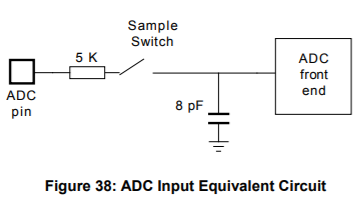
    Thanks for considering to use a Texas Instruments current sensing solution.  If I understand your issue correctly, you notice an oscillation on your INA180 output for a DC current condition of 1 Amp across your shunt resistor. From what you have told me I am assuming your INA180 is connected directly to NXP 5168/5169 ZigBee SOC ADC without any filter in between. This actually is expected behavior due to the ADC. The NXP device’s ADC uses a successive approximation ADC which has an equivalent internal sampling circuit like the one shown below (section 17.1.1 of the datasheet). Essentially every time sampling initiates and the internal switch turns on there is a large pull of charge on the load feeding into the device, because the sample and hold capacitor at turn on is either completely or nearly drained. As such for these kinds of ADCs you typically need either a very high bandwidth amplifier to connect directly to the input or you need a charge bucket filter between the amplifier output and ADC input. Yet another thing you can do to improve the sample quality is increase the acquisition time to give the input more time to settle after the ADC switch turns on.

    For more information on this topic, I would recommend watching the following video if you have time: https://training.ti.com/ti-precision-labs-adcs-intro-to-sar-adc-front-end?cu=1128375. Although it talks about our ADCs the concepts should still apply to your NXP device. Also on that page, we also have an analog engineer’s calculator that can help you calculate the values for the RC filter. The details of how you could use that calculator are near the end of that video.

  • Hi Spencer,

    I agree with Patrick: You should insert a RC filter between the output of INA180 and the ADC input. This issue is even mentioned in the datasheet of INA180. Please have a look at figure 45.

    Inserting a RC filter is a standard procedure when connecting to a successive approximation ADC and the design recommendations in the datasheet of ADC should be followed. The RC values differ from ADC to ADC.

    Kai