This thread has been locked.

If you have a related question, please click the "Ask a related question" button in the top right corner. The newly created question will be automatically linked to this question.

INA128: Output Voltage for RG Pins

Part Number: INA128
Other Parts Discussed in Thread: TINA-TI, INA118

Hi,

The output voltage for RG pins is -612.24mV at gain = 1 when simulating the dc analysis for INA128 with TINA-TI spice model but I think that the expected value is 0V.
Could you please tell me that reason about it ?
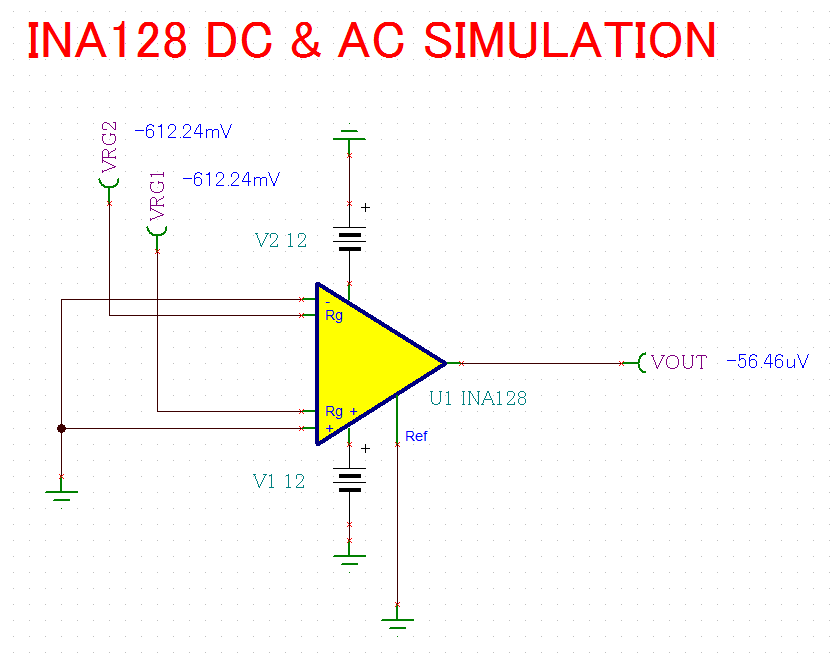
Best regards,
Kato

  • These INA type products have internal node limitations depending upon Input CM voltage, REF voltage, Gain, and differential input voltage.
    This link will allow you do download a powerful INA Calculator that can check to see if you are operating your design in a linear region of operation.

    www.ti.com/.../ina-cmv-calc
  • Hi Tim-san,

    Thank you for your response.

    I would like to know the voltage for RG pins at gain = 1(RG pins are NC), not the input/output dynamic range.
    Could you please tell me the voltage for RG pins on the following condition ?
    I think that the internal amplifiers for A1 and A2 is the voltage follower, so the expected value is 0V.
    However, the voltage for RG pins is -612.24mV when simulating the dc analysis.

    V+   = +12V
    V-   = -12V
    VIN+ = 0V
    VIN- = 0V
    REF  = 0V
    RGs  = NC

    Best regards,
    Kato

  • Look at INA118 datasheet for a better detailed description of this instrumentation amplifier architecture used in the INA128. It will explain why the RG pins look like -0.6V below GND. The PSICE model is close tot he behavior of the real part.
    If this answers your questions for now please check the “Customer Thinks Resolved” button. If in the future you have additional question you can re-post them or submit a new E2E post. Thanks.
  • Hi Tim-san,

    Thank you for your explanation.

    I understood.

    Best regards,
    Kato