This thread has been locked.

If you have a related question, please click the "Ask a related question" button in the top right corner. The newly created question will be automatically linked to this question.

2 sensor signal commons - offset (IN-AMP) or isolate (ISO-AMP)?

Other Parts Discussed in Thread: XTR115, XTR116

Hi. I have an interesting sensor design problem I'm looking to solve with either an analog isolating amp (which I have no experience with) or an instrumentation amp (which I have some experience but not much).

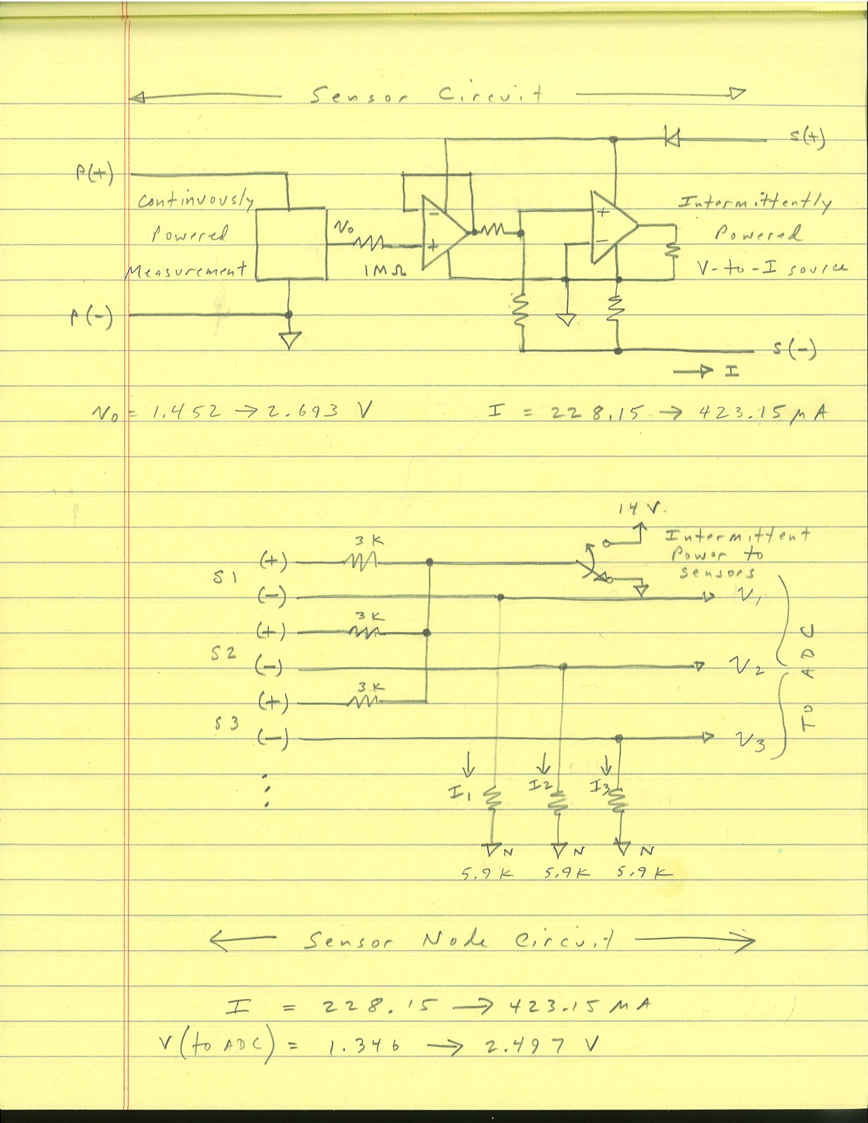
Sensor circuit has 2 parts:

Continuously powered (P terminals) measurement, and intermittently powered (S terminals) signal current source. The continuously powered circuit has regulated Vdd (5V) and outputs the signal Vo = 1.452 → 2.693V. The intermittently powered (8 to 11V unregulated Vdd) V-to-I source circuit converts Vo into a sub-milliamp current signal I = 228 → 423µA. 

When it’s time to take sensor measurements, the battery powered Sensor Node simultaneously powers all connected sensors at their S terminals, causing a signal current to flow in each sensor loop. Since each sensor signal current is different, each sensor’s S(-) terminal voltage is different. Note that there is no access to the Sensor Node internal circuit common. 

The sensors require separate, isolated power at their P (continuous) power terminals because connecting a common DC power source to multiple sensors would interconnect their internal circuit commons, preventing their V-to-I sources from operating independently. 

I want to change that. I want to power multiple sensors P terminals from the same DC power source. To do so, it seems to me I need to break the sensor signal common into two: one common (continuously powered circuit) will be at the same potential among all connected sensors; the other (V-to-I source internal common) will move up and down (∆V < 1.6V) with the signal current.

One thought is to insert an analog signal isolator at Vo so each sensor’s continuously powered and intermittently powered sections have separate, isolated signal commons. Does TI offer such a product which will operate within my two Vdd ranges? Recommendations? An additional requirement is the output stage must power up and stabilize within a couple mS.

Is there another way which doesn’t require isolating the sensor’s two signal commons?

Each V-to-I source internal circuit common’s voltage potential (relative to the Sensor Node internal common) varies less than 1.6V. Can an instrumentation amp’s ability to level shift accomplish this? I’m picturing a differential Vo with –terminal connected to the V-to-I source internal circuit common, and +terminal connected to the V-to-I source voltage input buffer. This approach seems somehow possible but I’m uncertain how to keep this “floating” differential Vo within the correct voltage range relative to the in-amp inputs.

  • Hi Kris,

    I don't fully understand what your sensor looks like or what needs to be isolated in the circuit above, but as shown the V-I circuit you have implemented has multiple sources of current error that likely need to calibrated out and is very sensitive to changes in the load. You may consider using a topology like this: 

    Kris OPA192.TSC

    I don't think this is going to work with an instrumentation amp because you always have to provide a dc path to ground for bias current and this seems like it is going to eliminate the effective isolation you are going for. 

    For ISO amp recommendations you will want to talk to the isolation amplifiers group. We can redirect you to their forum if you'd like to investigate this option.

  • Hi Zak. Thanks for your response and let me fill in a bit more background:

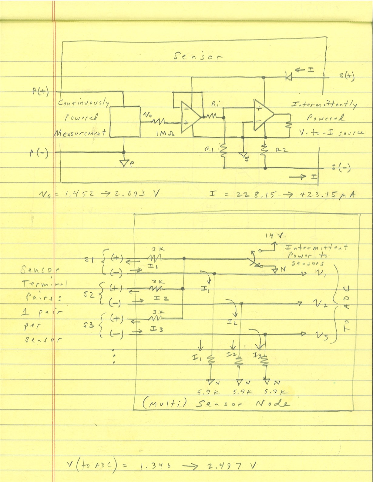
    Here (below) is the schematic diagram with boxes drawn around the Sensor circuit, and the Sensor Node circuit.

    The Sensor is a separate, self-contained entity with its own housing and 4 external terminals P(+), P(-), S(+), S(-). An external
    supply (not shown) powers the Sensor continuously powered measurement circuits from P(+) and P(-). The Sensor connects to the Sensor
    Node with its S(+) and S(-) terminals.

    The Sensor Node is a separate, battery-powered, self-contained entity with its own housing and multiple 2-terminal sensor
    connectors. Each sensor connector connects to a separate, external sensor, by cable. The Sensor Node's internal circuit common
    (labeled N) is not accessible. Each sensor connector open-circuit voltage is 14V maximum (when energized).

    A system consists of one Sensor Node and several Sensors. Each Sensor is connected to a sensor connector on the Sensor Node (S
    terminals). Each sensor in the system must also receive power (at its P terminals) from an external power supply (not shown).

    The Sensor has 2 internal circuit commons: labeled P and S, which when connected (as they are now) requires that each Sensor's
    external P supply be electrically isolated every other sensor's P supply. I want to change that requirement. I want the system to
    work with a single supply powering all the sensors.

    There are multiple sensors which feed their current signals into the Sensor Node.

    The Sensor Node was originally developed for 2-wire 1uA/K temperature sensors who's 223 - 423uA loop current (intermittently powered
    current loops) is insufficient to power this other type (not temperature) sensor who's circuit I show. Also, the nature of the
    measurement circuits in this other type sensor requires them to be continuously powered, so I developed the circuit I depicted with
    2 parts (continuously powered measurement, intermittently powered V-to-I source.

    The sensor circuit works very well, including the V-to-I current source which is insensitive to loop resistance, so long as there is
    adequate voltage drop across the terminals S(+) and S(-). With the dual op-amp I use, the main error source is the op-amp Vos, which
    is adequately low. This 2-wire V-to-I loop powered current source is a tried-and-true circuit which forms the basis for TI's
    XTR115/116, etc. Where V is a signal voltage (relative to the S common), I = (V/Ri)*(1 + R1/R2).  Please explain your circuit topology and what it's doing. 

    Assuming I keep my V-to-I current source as-is, I'm looking to change the circuit so I can supply the continuous power terminals (P+, P-) of multiple sensors from the same supply.

    Consider the signal current loops (sensor S terminals connected to Node S terminals). The sensor's internal V-to-I source circuit
    common (labeled S) voltage (relative to the Node's internal circuit common, labeled N) will go up and down with that sensor's loop
    current. Since the Node has terminals for multiple sensors, each connected sensor's internal V-to-I source circuit common (S) will
    be at a different potential according to its signal current. If the continuously powered measurement circuit common (labeled P) is
    connected to the V-to-I source circuit common (as it is now), a separate isolated/floating power source at each sensor's continuous
    power (P) terminals is necessary.

    That's what I want to change. I want to change the sensor circuit so that multiple sensor's continuous power (P) terminals may be
    supplied from a single supply, within this system (of multiple sensors connected to a single Sensor Node).

    Given the loop resistance values (3k + 5.9k) and signal current (I) range (228 to 423uA) and V-to-I source resistances, the V-to-I
    source circuit common (S) potential (relative to the Node circuit common N) can vary only about 2.1V maximum (my previous 1.6V was
    incorrect).

    So in the sensor, I want to separate the measurement circuit common (labeled P, shown connected to P-) from the V-to-I source
    common (S, shown connected to dual op-amp V- and one -input) thereby allowing each sensors V-to-I source common (S) potential to
    vary (2.1V max) with the loop current while all sensors measurement circuit commons (P) are interconnected. To accomplish this, in
    the sensor, I want to insert something between the measurement circuit and the V-to-I circuit which will translate the measurement
    circuit common (P) referenced Vo signal to the V-to-I source circuit common (S) referenced input buffer. It's a level shift within
    the sensor from one common (measurement circuit) which is the same in all sensors, to another common (V-to-I source) which will vary
    from sensor to sensor according to the sensor S loop current.

    The most straightforward method (to me) is to use a precision isolating amplifier and I'd love recommendations.

    My other idea is not to isolate, but rather just do a level shift from input to output. I base this possibility on what I see when I
    look at this whole system:

    We have the Sensor Node internal common (N) which is the lowest potential of the system. We have the Sensor Node S(+) terminals
    which are maximum 14V (open circuit) above the Sensor Node internal circuit common. Between those two potentials are the sensors V-
    to-I source internal commons (S), which are all within a 2.1V band. We also have a single DC supply powering all the sensors
    measurement circuits (all sensors share the same measurement circuit common P). So I need an input-to-output voltage shifter in each
    sensor to allow for each sensors V-to-I source common mode variation (2.1V max). Because this variation is relatively small, it
    makes me think isolation shouldn't be necessary ... what's hanging me up is what will keep the sensors measurement circuit common
    from floating up or down and railing the voltage shifter input.

  • Kris,

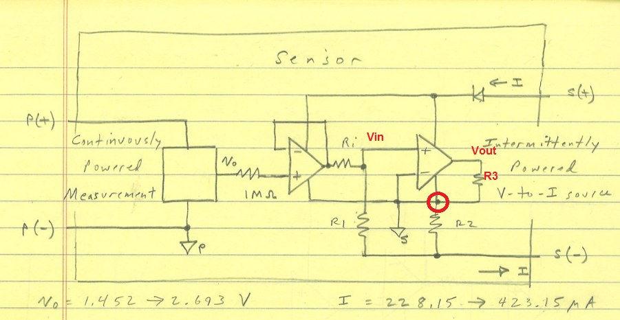
    Before we may talk about all other requirements like isolation between different channels, we need to straigten out the basic design of your current source - the way you have it set up right now balances output current vs output voltage on the blade of a knife, putting several constrains on the ranges of allowable Vin and Iout.  It also makes it difficult to calculate the total output current because it is a function of Vin, Ri, R1, R2, R3, and (S-).

    Shorting the input and output to a negative rail across R3 resistor (see above) is a really bad idea since it now requires certain minimum output current in order to assure that the output is far enough above negative supply to assure op amp linear operation.  Also, addition of currents thru R1 and R2 contributes to the total output current and is now also a function of Vin and s(-).

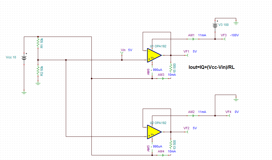
    Please consider using a basic configuration shown below where current sourced by each op amp is simply a function of supply voltage, Vcc, Vin, and load resistor, RL - see below.  For Vcc=10V and Vout=5V, Iout=(10V-5V)/500ohm+IQ=10mA+IQ.  The configuration shown below allows you to easily change the output current by changing the ratio of R1/R2 or changing RL.  Notice that unlike in your design, in this design Iout is NOT a function of s(-) voltage.  AM1=AM2=11mA for VF3=100V and VF4=0V.

  • Hello Marek,

    Yes, you are correct that the circuit requires a minimum output current in order to assure that the output is far enough above negative supply to assure op amp linear operation, but I don't think it is a bad idea since I ensure that happens. 

    Vi (driving the other side of Ri than your label) must exceed a minimum value to drive the op-amp output positive, adding sufficient current to the op-amp quiescent current (< 50uA in my case) to close the loop, which it does: Vi (measurement circuit Vo in my schematic) = 1.452 -> 2.693V.

    In normal linear operation, the output current is not a function of R3 or S-. High differential gain maintains Vout, stabilizing the current through R2. The op-amp + terminal is virtual ground (relative to S ground).

    To understand, put Vi on the other side of Ri (from what you show).

    The current through Ri and R1 is Vi/Ri. High gain and negative feedback adjusts the op-amp output volts for i(op-amp output) = V/R3, forcing the negative input to near the same potential as the positive input, so R1 and R2 have the same voltage across them:

    I(R1) = Vi/Ri;

    V(R1) = V(R2), so I(R2) = V(R1)/R2 = (Vi/Ri)*R1/R2;

    I = I(R1) + I(R2) = (Vi/Ri)(1 + R1/R2)      

    I chose R3 according to my operating parameters (available voltage swing per the op-amp, loop voltage, loop voltage drops, R2 and loop current). 

    See the TI XTR115/XTR116 data sheet. It's the same current source circuit, only my much lower loop current/power doesn't warrant the external transistor, so I use a resistor R3 instead.

    XTR115 proper operation isn't any more knifes edge than mine and it's current isn't a function the external transistor used or it's -pin (Io) voltage. XTR115 current is a function of Vin, Rin and the internal R1 and R2.

    I've built and tested and operated this circuit in real sensors, outdoors, Minnesota, on our building roof, year-round, rain, shine, snow, sleet, extreme heat and cold. It is precise, accurate and stable. 

    Your circuit has Iout a function of Iq and Vcc ... 

    xtr115.pdf

  • Hi Kris,

    First thank you for including the level of detail that you have in this post. I've spent some time looking at this in sim and I think this is really the same problem we face with multiple channels of 2-wire XTR circuits and the only solution I've found is to use an isolator. At face value and even in simulation, it seems plausible that level shifting would be able to achieve what you are after. But I think as you have pointed out, you don't know where your commons sit relative to one another and you risk floating outside the valid input range. If the front end is powered outside the loop then you also risk running into the output limitations of the device. I believe the only approach that guarantees proper operation is going to be isolation. That being said, if you do manage to find a functional alternative I'd be eager to see it and could certainly look over it for you.
  • Hi Zak,

    Thanks for your response. I think you're on to what I'm looking to do, have encountered similar applications and have considered the same two basic solutions. 

    Regarding the isolator approach, what did you use?

    Isolating amplifier? If so, I'd love a recommendation. Does TI offer anything oriented towards sensors (precision)? 

  • Hey Kris,

    The ISO7310 is something commonly used with XTRs, but on second thought I don't think this approach really works for you either because of the low current levels you need. The quiescent currents contribute to your loop current and consequently you need all of your circuitry to consume less quiescent current than the minimum desired loop current. Most isolators I've seen consume 1mA+, though I must admit I do not support those devices. I can certainly move this to the isolation team if you'd like. They may have a clever solution around this.

    The problem with this circuit is that even though the output is shifted inside the supply range, you don't really know where the input is and it is likely going to slam into one of the rails because of the bias current. You have to provide a path to neutral to avoid this, and I don't believe that is possible in your present configuration. It's a little misleading when you simulate this because it seems to converge to reasonable values, but I think this is spice providing a high impedance path to neutral, which ends up being sufficient to stop the amp from saturating, though this path doesn't actually exist in your circuit. If you were to simulate the same circuit with a higher bias current device, you would find it indeed slams into the rail.

    Sensor Level Shift B.TSC

    If you can reference the 5V supply to one of S references in your circuit then I think this might work, but at that point front end is no longer continuously powered. Something like this might work: 

  • Kris

    We haven't heard back from you so we assume this answered your questions. If not, post another reply below.

    Thanks
    Dennis
  • Hi Dennis,

    Sorry, I've been out of office for a few days.

    Regarding isolation amps, yes, the output amps required power looks to be a show stopper. 

    As for the other approach, I will study Zak's last post and may follow up, but for now I think we're done.

    Thanks to all!