This thread has been locked.

If you have a related question, please click the "Ask a related question" button in the top right corner. The newly created question will be automatically linked to this question.

INA225-Q1: High Current trough Vin+ & Vin- in normal running - Possible cases?

Part Number: INA225-Q1
Other Parts Discussed in Thread: INA225, INA240

Hi Dear E2E Forum,

I'm using the INA225-Q1 device into a bidirectional applications having the following configuration conditions:

VS : 5V, ±5% accuracy

Vref: 1V8 ±2% accuracy

Gain configuration: 50 ( GS0 = "GND", GS1 = "Vs")

Shunt resistor: 10mR, ±1% tol

Measured current range: ±3A 

Common mode voltage: 7V to 30V

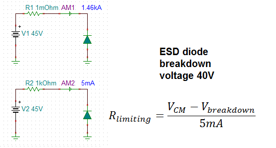
Phenomena observation:  During efficiency evaluation, there was observed that the INA225 device was getting hot up to 150ºC ( no external input resistance used). I placed input serial resistance of 1k through each differential in lines ( 1k per each line just to limit the current, I'm aware that the accuracy is affected). The current was lowered, the output of INA was also working ( expected well with an -30% accuracy in comparison with current loop measurement).

After this trial, I externally injected voltage through each Ni+ and Vin- and the current was increasing very high ( Vin+: 30mA  at 2.5V using a 50R series resistor, The current drawn from Vs was 30mA, on Vin- i measured 0.6mA at 2.5V using 50mR series resistor, in this case, the current was very low). So the current of Vin+ is affecting the supply current... 

I have the following questions:

1)  What could lead to this kind of behavior? (  in some conditions I may have some small inductive pulses higher than specified VCM, for a very short time)

2)  What is the maximum accepted current in case of VCM achieved .. 10R to 50R is enough to limit the clamping current?

3) What could be more or less affected internally...? ( I saw some bias network between Vin + and Vin-, before the internal series resistor) 

4) Is it possible to have the device functional if the input lines are affected? (I'm very surprised that even in that worst conditions the output of INA225 was reflecting something approaching the reality).

5) Do you have any design configuration of INA225 in inductive load applications in a bidirectional application?  ( H Bridge applications reading the inductor/motor current in both directions not as low or high side configuration)

  • Hello Natanael,

    Thanks for considering to use the INA225 in your system.

    1. From what you have said about externally injecting a voltage on VIN+ and VIN-, you probably have destroyed the part as the 30mA is substantially higher than the typical input bias current of the part over the entire common mode voltage range. I think if you perform the same test with a fresh part you can confirm this.

    While the internal ESD structures are designed to protect the device from ESD events that inject large voltages onto the device, these events are of extremely short duration. Your inductive transients although short to you, may still be an order of magnitude longer than a typical ESD event and as such may allow for the ESD to sufficiently heat up and experience thermal damage.

    2. If you want to limit the current solely with a series resistor to your input pin, you will need a fairly large one depending on how far above the rated common mode voltage you plan on going. Below I give a simple example. The top shows what current will be sunk assuming there is only board trace resistance, while the bottom example shows how to sink only 5mA given max transient VCM is 45V.

    3. & 4. Device failure can take many forms. It is possible to have a slow degradation in performance from exceeding device specifications. All are expected to fail eventually when device specifications are exceeded. When the ESD structure breaks, it can randomly cause shorts or open circuits which may not always consistently show the same failure behavior.

    5. For the INA225, I am not aware of a specific appnote or TI design that involves sensing inductive loads in an H-bridge. However, I will check with my team to see if in fact we do have something.  What switching frequency are you using? The one device that we typically promote involving inductive loads would be the INA240. That is analog output device. We have some information on inline sensing here as well as an example here.

  • Hello Patrick,

    Thanks for your prompt feedback! Below you have the missing inputs of your considered point.

    Related to:

    1) I already ordered fresh samples, I expect your mentioned behavior

    2, 3 and 4) I would use 1K as in inductive load enhancement, I don't have time to introduce INA240, I have design freeze in 1Week. The problem here is how controllable is the gain error factor in function of input resistance ( see my draft evaluation from attachment assuming an input resistance from 0.1 to 1000 ohm). May I use my calculation a an gain error factor compensation? EG: if using 1k that the ADC_CURRENT maiybe compensated with  aan correction factor of  Iout*(1+0.451) ? How accurate may be that... ? How stable/ Controllable is the input resistance  RINT ?

    5) I would really use the INA255, it's already in my data base and used on other projects..

  • Hello Natanael,

    These Rint impedance is 40k with a tolerance of 15%. So your gain error may range from 45.1% to 45.3% and you should be able to calculate this using the formulas you posted above.  As you intend to compensate in your ADC reading and account for the change in gain, you should be ok.  However, do not forget that there are other sources of error.  Most of the other sources will only matter for low currents though.  If you are unfamiliar with error from CMRR, PSRR, and offset, I would recommend looking at the following training series here.