This thread has been locked.

If you have a related question, please click the "Ask a related question" button in the top right corner. The newly created question will be automatically linked to this question.

INA240: Pspice model V/A two shunt values

Guru 55913 points
Part Number: INA240

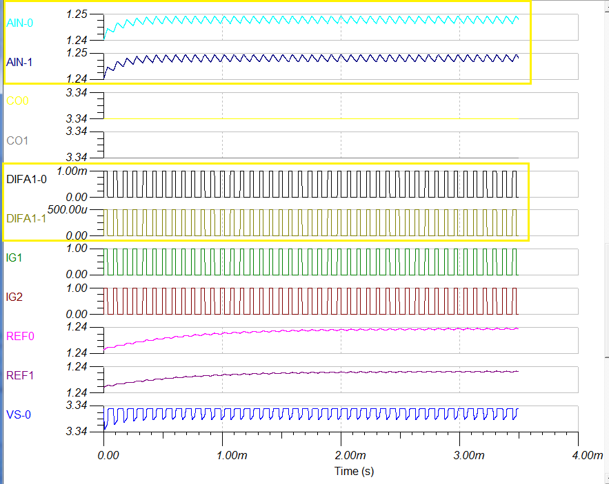
Analysis of INA240-A1 in two transient models; 1mohm shunt on one INA and 500uohm shunt other INA Pspice circuit. Oddly both models produce same output signal plot (1.24v/1A) shunt current.

How can output amplitude plot the same peak voltage if 1mv/A shunt on one, 500uv/A shunt on other INA? Is there Tina options switch change require to evaluate each Pspice model separately? Have I missed point shunts uV/A value controls amplifier output level relative to the REF1+2 voltage level? What have I done wrong to evaluate two different V/A shunts.

  • Hi BP101,

    Both circuits have an output offset, by way of the REF pins of 1.24V. In order to get the gain, you need to subtract this offset from the output. Once you do that you’ll see the correct gain for both circuits. Also, you may want to slow down the frequency so the output resembles more of a square wave instead of triangular.

    If you still have difficulty/questions, please attach your TINA circuit. It will help us understand your question better/quicker. In addition, it helps tremendously if you state clearly what the expected result is and what the actual simulation result is etc.

    Regard, Guang

  • Hi Guang,

    That's the point, there should not be the same output amplitude for 1A shunt current from two different shunt R values. Look again, agree the REF sets 1.24v output on each INA but outputs should not have the same amplitude relative to the shunt value. The outputs differ at 8 amps shunt current but not even close to bench circuit shunt pulses peak A1 (4mv) with A2 (100mv) average @7.9-8.4A from DC supply with 750uV/A bar. According to Tina the 500uv/A shunt should see 5mv rise @8A. The bench capture 1000 SPS deep reduces the higher frequency rolling peaks going well beyond 100mv across shunt.

    Why would we want to slow down the frequency representing real world PWM @80us inductive periods with lots of ripple/ringing? Is not the idea to make Tina results be as close the actual CUT on test bench? Not really matter since the bench circuits shunt CMMV has much greater mV gain than Tina shows in any of these plots A1 or A2 devices.

  • Hi BP101,

    To your first paragraph – I don’t know how you did your test bench, but I know this, if you built your bench setup as your TINA circuit shows, you’ll NOT observe the correct gain with the PWM excitation you have in the schematic. Simply put, the circuit will not work as you expected. This will be explained below together.

    To your second paragraph – The circuit has a bandwidth of 1.5KHz due to the filtering in your circuit. Your PWM is at 12.5KHz, far exceeding the system bandwidth. The output is not going to be an accurate  representation of the input. This is exactly why I asked to slow down the PWM in my previous post.

    Here is a plot with 8mS PWM, instead of 80uS. The two outputs and their difference are spot on.

    Regard, Guang

  • Guang Zhou said:
    The circuit has a bandwidth of 1.5KHz due to the filtering in your circuit. Your PWM is at 12.5KHz, far exceeding the system bandwidth. T

    The A1 400Khz bandwidth CMMR @12.5Khz=103db figure 12 of datasheet. The SAR filter R1/C7, R17/C18 represent only the SAR input capacitance are not part of the 15n input filter. If your idea was true the bench circuit would not produce the signal shown below which incorrectly has REF1+2 (1.225v)  added into INA output gain, opposed to Tina transient simulation models. Notice top INA (1mv/A) is 9mv/A and IG1/2 are 9 amps  deviates from the actual 8 amps peak being verified on the test bench.

    Imaginary math below capture produces correct 63mv (6.2A) if we "manually" subtract REF (y2) from (dy) as you mention first post. Final amplitude (y1) is incorrect as the INA is supposed to subtract (dy) REF not add it to 63mv (x20) gain. The INA output should be 1.3v 1.228v for 63mv @6.2Amps but not 2.7v otherwise INA is simply acting like an OPAMP being incorrectly called a current monitor.

    Something ain't right as we have more than 1 INA in the bench circuit. Fact is we have 3-A1 on test bench all 3 REF are being added into the amp gain. Ohms law states the parallel REFS reciprocal of the added reciprocals may in fact plague REF1+2 of more than 1 INA tied to a single voltage reference even with 6.8k series isolation resistors. So the internal REF resistors are being divided (parallel) with other INA amps in the very same circuit. Tina model seems to show the same results in a different way. Otherwise how can the INA higher output potential (REF added) be explained other than by Ohms law?  

  • Agree removing the SAR internal filter from model set IG1/2 back to 1 amp, C5/C2=1nf the transient results are more consistent @1amp. Also noticed a IG1, IG2 were set above 1 amp the results with SAR internal filter in model more consistent.

    Yet the test bench A2 or A1 gain even with 1n or no output RC at all incorrectly adds REF1+2 (1.225v) into INA output gain. So the transient model is not showing the REF1+2 being added into the output gain of the 3 bench INA in a shared parallel REF formation. It doesn't matter even if output filter is omitted, the +1.225v shared REF always gets added into the output gain of the 3 test bench INA under analysis.
  • Hi BP101,

    To your first paragraph – I take it that you’re good with the explanation.

    To your second paragraph – Is this a new problem? I don’t see three INA240 in the schematic. If there is a voltage on the REF pins, this voltage will be added to the INA240 output, that is the way how the device works and it has nothing to do with gain. If you’re expecting a behavior other than this, please attach your TINA schematic together with the expected results (such as input/output). It works better than long word description.

    Regard, Guang

  • Guang Zhou said:
    If there is a voltage on the REF pins, this voltage will be added to the INA240 output, that is the way how the device works

    That would be an incorrect assumption as the REF should only set the floor of the output signal and the shunts + amp gain (10mV/A) is added to that floor. Tina transient analysis plot show such even with only two INA.

    The problem is Tina analysis is not plotting the bench effect of how multiple INA sharing the same REF being (incorrectly) added back into the gain when multiple INA exist in the same circuit. Ohms law "reciprocal of the added reciprocals" for parallel REF's is not being evaluated during transient analysis. The bench result for 6.2 amps should be 1.3v as Tina plots and not 2.7v as bench shows as that too violates our Tina model even for two INA sharing REF voltage source.

    If you check the scope capture above plain to see +1.225v REF was added to the +1.225v floor + 63mv making 2.7v, should be 1.3v.

  • Hi Guang,

    Adding 75k in series with each of the INA REF1+2 floated +1.225v reference up to 1.45v on test bench. However it becomes more apparent as the PWM duty cycle increases so does the INA output amplitude increase upward beyond the 1.225v reference being added to shunts 10mv/A output signal. That attribute is not showing up in these simple Tina transient models. With A2 we had to add capacitance up to 39n ADC filter to compensate for the same odd attribute may have made it worse just so the SAR could properly acquisition the signal.

    That filter created longer SAR acquisition times in a nice saw tooth for A2 higher gain and it too became clear something was not quite right REF1+2, so installed A1's on our test bench. The PWM duty cycle speed is somehow causing the INA output amplitude to increase magnitude beyond what it should thus making it appear as if the REF is at fault. Past tried a sweep generator in Tina transient analysis but could not duplicate the shunts wave form as the duty cycle increases with motor speed order to simulate the same INA output being captured on test bench. That step seems vital to correct the excessive INA output amplitude going beyond the actual measured shunt 500uV/A INA output 1.305v (80mv) @8amp.
  • Guang Zhou said:
    If you’re expecting a behavior other than this, please attach your TINA schematic together with the expected results (such as input/output). It works better than long word description.

    It was included in the first post Tina model of the bench circuit.

    Guang Zhou said:
    If there is a voltage on the REF pins, this voltage will be added to the INA240 output, that is the way how the device works and it has nothing to do with gain

    Perhaps you meant to say the REF sets the output bias and infers the signal floor. So as the bias floor (REF) is lowered so should the output magnitude lower respectively to that of REF. That is what Tina plots show in transient analysis but the test bench deviates from that theory in reality. Note the function generator was running background attached model @12.5kHz. The point was not about the RC output filter rather the two INA being in the same circuit. The original INA240 model DC plots changed after A2,A3,A4 were removed from the same analysis some time ago.

    Besides the output RC filter of the ADC has nothing to do with the shunt resistive value in transient analysis. Once the shunt bias reached minimum of 90uv in each case the two outputs should not have been at the same level. 

  • Update:

    This weekend tested both test bench, Tina model REF2=GND, dividing REF1 (1.225v) reference internally (0.6125v), output bias respectively. Tina model indicates that change would lower 2.7v shown in scope capture above to roughly 2.0875v.

    That too produced incorrect test bench current measures respectively in either output case of a 75 amp or greater full ADC scale. Yet also an indicator REF1/2 inputs have no direct impact to control the output signal magnitude respectively as Tina plots show they both should. Seemingly the INA datasheet has omitted certain laboratory test results that greatly impact the INA output magnitude in the presence of real world low side PWM shunt signals below 80v CMMV.