- Ask a related questionWhat is a related question?A related question is a question created from another question. When the related question is created, it will be automatically linked to the original question.
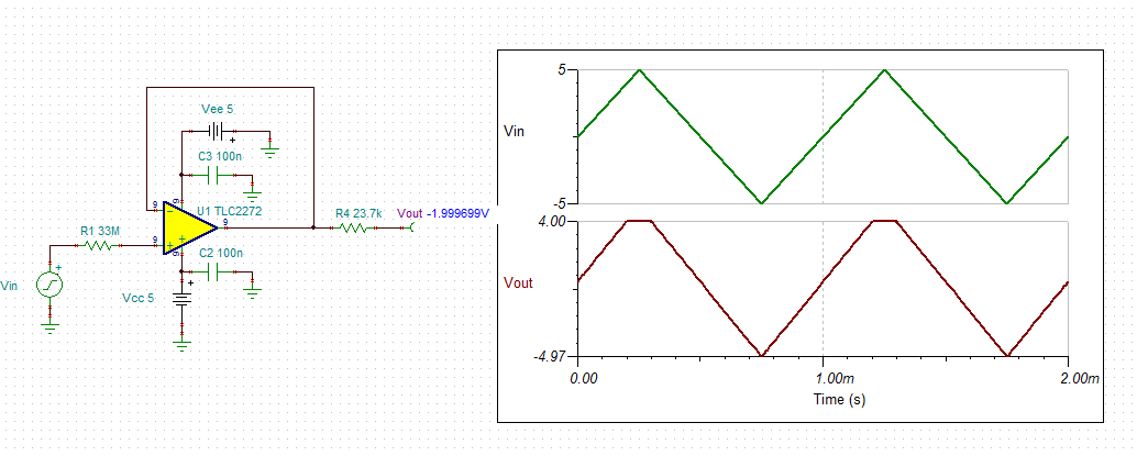
I am investigating a production issue for a legacy design where a tlc2272acpwr opamp is configured in a buffer follower configuration with the output tied to - and the + input is driven by a another opamp at -2.0V in series with two 33 megohm resistors in series. The voltage at the + input is -0.29V. The voltage rails are at +5 and -5V. The output connects through 23.7k to an ADC input. On passing boards the ouput of the tlc2272 and the input of the ADC is -1.48V. The test limit requires ADC input is no lower than -1.65V. On failing boards the voltage is -1.66 to -1.69V. The connections between the components in the circuit have been verified and the components have been swapped but the failing boards continue to fail and no incorrect connections have been found. The circuit was simulated and voltage on the input matched the output over the range the circuit operates. When the input of the circuit goes high (3.6V) the output matches it and the simulation.
Are there conditions where the opamp won't behave like an opamp and a buffer follower output won't follow the input?