This thread has been locked.

If you have a related question, please click the "Ask a related question" button in the top right corner. The newly created question will be automatically linked to this question.

INA250: INA250 defct with open REF Pin

Part Number: INA250
Other Parts Discussed in Thread: INA190

I'm using the INA250A4 with a power supply of 36V to measure high side currents up to 100mA .

- I used 100nF at the VS pin (36V constant power supply)
- SH+/VIN+, and SH-/VIN- are connected without any component, filter TVS diode.
- IN+ is connected to a variable OPV output of 0..36V
- IN- is connected to a load resistor

In the beginning I left the REF pin open (erroneously).
Is it possible that the INA250 can be "killed" by leaving the REF pin open ? because at the OUT
of the INA250 I always measure constantly 8mV independent from any current flowing through
the shunt...

Any comments welcome..

  • Hello Wolfgang,

    Thanks for considering to use Texas Instruments in your design. The device should be fine as long as the ref pin voltage is between 0V and the supply voltage as long as the supply is not greater than 18V. I presume if it was left floating it should stay somewhere in this range, however, I need to run a test to verify.

    As for the voltage you are seeing that is a bit odd. I would expect 80uV at most on the output if the input pins were at roughly the same potential from no load passing through the shunt. This offset I expect would be due to the voltage produced by the device offset current across the device shunt multiplied by the gain. As 8mV is considerably higher than that, the device may be damaged. I will test if it is related to a floating REF pin. However it is possible there was a transient at startup or during some periodic event that introduced conditions that may have violated device specifications.
  • Hey Patrick,

    The supply voltage is 36V (until now). So if the REF pin is floating it's possible that it's voltage becomes too high or ?
    I'll test now with the a new device where REF Pin = GND = 0V (the original intention of design:-) )

    And then I hope/think it should work.

  • Hello Patrick,

    Now the 4 INA250  I use in the design are working. In between I really think
    the other once had been killed by open REF pin while using VC=36V.

    I still have a small offset of some mV in my circuit, but I think this comes from a grounding problem.

  • Hi Wolfgang,

    as your input voltages are so close to the rated maximum input voltage of INA250, I would heavily recommend to add TVS at the inputs as discussed in section 7.4.4. Choose a TVS with a low leakage current. Even for the supply voltage I would consider using a TVS.

    Keep in mind that every inductive load can produce dangerous inductive kick-backs which can easily exceed the maximum input voltage range of such a chip. Even a simple cable with its cable inductance can provoke this. So, from my experience these above recommended TVS are a must in such applications.

    It's a bit improbable that leaving the REF pin unconnected results in a damage. But I wouldn't say that it's impossible, especially when your input voltages are such high or are even contaminated with transients.

    Kai

  • Ok, the output of the circuit is already protected with TVS diodes, you are right I will protect the Inputs VIN+/VIN- also.
  • Hello,

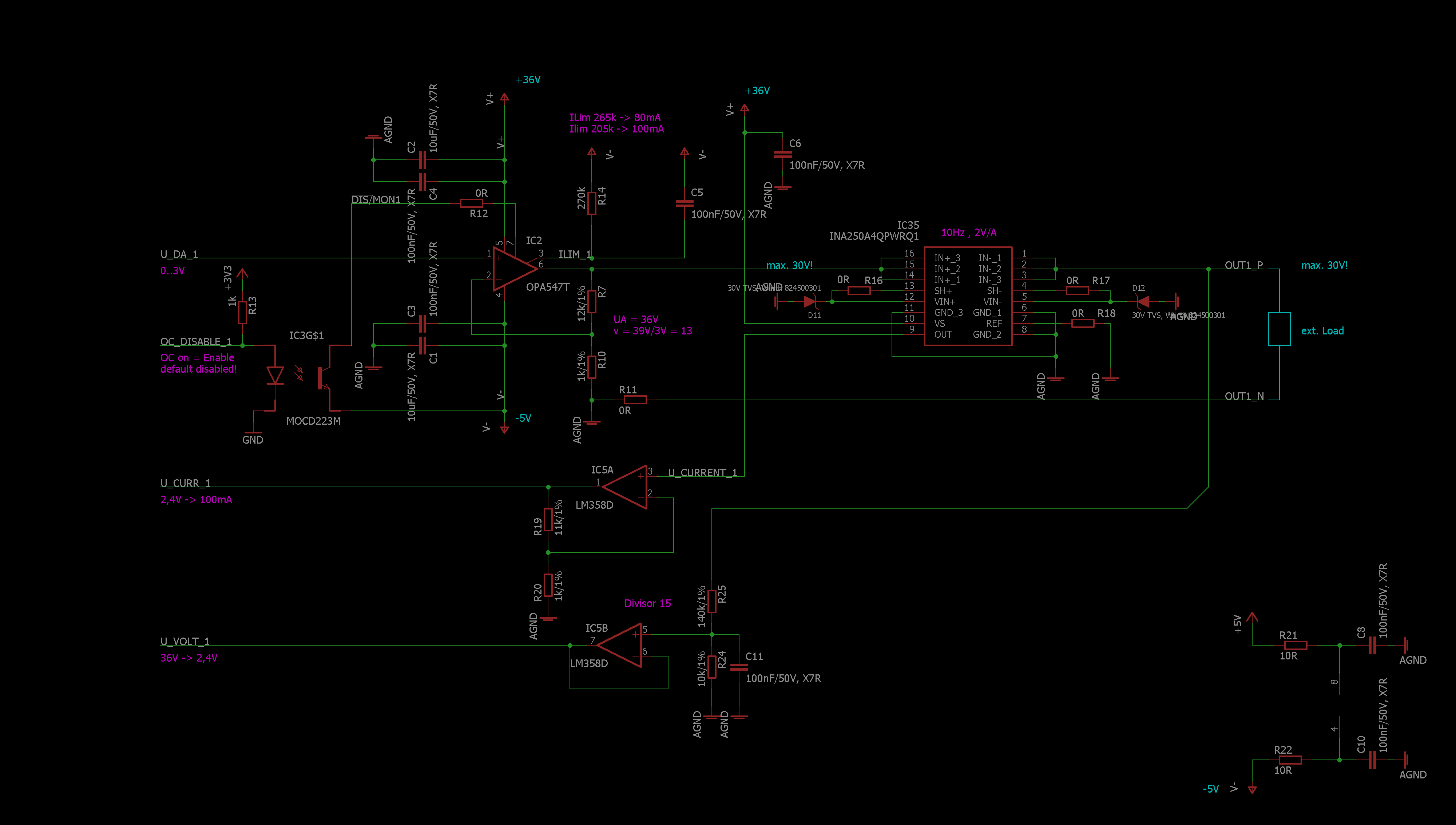
    Attached you find the circuit where the INA250 is used. It's working, but I still see an offet of around 30mV
    at the OUT of the INA250 while NO current is flowing.
    - The effect is the the same with or without the TVS Diodes, so they have no negative effect.
    - The voltage measurement at R25 is also not the problem, because there is only a max. current of 200uA at 30V,
      (also R25 disconnected makes the same problem)

    So with U_DA1 set to 0V I see ~30mV at the OUT of the INA250. This voltage rises with rising U_DA_1.
    The maximum voltage at the INA250 IN+ is 30V. The current calculation readed from the U_CURR_1
    tells me 3mA .. 15mA in the range of 0..30V at the INA250 resistor. NO load is connected for that test.
    If I connect a load the measured current of the INA250 is ~4mA higher than measured by an amperemeter.

    The voltage reading at U_VOLT_1 is always correct ..

    Any idea ?

    AGND and GND are ground planes on the board

  • Hi Wolfgang,

    the output of INA250 cannot fully go down to 0V. See the "voltage output" specifiction on page 6 of datasheet.

    Kai
  • Thank you for that information... So I have to set REF to i.e. 100mV and use this as zero point or ?
  • Yes, that would be a remedy.

    Kai
  • Ok I now use a 51mV at the REF Input of the INA, and the multiplier amp is set to 9,2, otherwise the 0mA Offset Voltage
    at the OP Amp Output is too high.

    But there is still this problem:

    With no load connected the U_CURRENT_1 ( and U_CURR_1) rises much more than I would expect with voltage measurement load
    of 150k (200uA at 30V).

  • Hi Wolfgang,

    increase a bit the REF voltage to have some headroom. Vref = 100mV is better then Vref = 51mV.

    And you cannot accurately measure 200µA when the offset current (RTI, referred to input) of INA250A4 is up to +/-20mA. Please see page 5 of datasheet.

    Kai
  • Hmmm the offset current is really high. The 200uA leakage current by the voltage measurement is not the problem but the
    offset current... Is there better amplifier existing to measure up to 1.. to 100mA ? This device is made for up to 10A, and I only need 100mA.
  • Hi Wolfgang,

    do you need the integrated shunt resistor at all?

    Kai
  • Hey Kai,

    This is not a "must" I could also think about a discrete diff. amplifier with shunt.
    I thought about to use the INA250 because of it's high integration and accuracy. But obviously I did not read all
    it's problems :-) If possible I'd like to find now an "INA" which is capable to measure 0..100mA at a max. of 36V.
    The shunt R could also be 20..25mOhm.

    If there is no replacement available which fits to the current layout I could also think about a low side measurement, then the
    36V are not needed, but this means definitly a new pcb layout is needed.
  • Is there any package compatible INAxxxx available which is better for measuring only 0..100mA with 0,5mA accuracy ?
  • The REF voltage was not stable enough, this is why the OUT voltage was rising with rising Voltage at the shunt...

  • Hello Wolfgang,

    If you are trying to measure really low currents, our best device is the INA190. It has the lowest input bias current and lowest offset voltage. For the most resolution I would recommend the 500V/V gain option if you intend to use a 20mohm shunt. For this device you will also need to buck down the supply voltage.
  • Hey Patrick,

    Thank you for your information. I think in the next application the INA190 could be used
    For now I reached now my target. I can measure 0..100mA with an accuracy of 0,5mA which is enough for me.

    The main points I learned to reach this :
    - the REF must be at > 50mV (in my case 64mV), otherwise low curents are not measureable
    - the REF must be very stable (OP buffered 60mV reference).

    And one point is very important: The INA250 outputs 0mA at 0V and 6,6mA at 30V with NO LOAD connected (this is linear between
    0..30V). meaning an error of 0,22 mA/V.
    If I use this "calibration factor" to correct the current measurement, everything is fine.
  • Hi Wolfgang,

    please also keep in mind that the offset current (RTI) shows a temperature drift of 25µA/°C typical.

    Kai
  • Hello Wolfgang,

    Sounds like you were able to to resolve your issue. However, if you still need any further support feel free to respond below.