This thread has been locked.

If you have a related question, please click the "Ask a related question" button in the top right corner. The newly created question will be automatically linked to this question.

TLV171: TLV171 Supply Considerations For A Electronic Load Project

Part Number: TLV171
Other Parts Discussed in Thread: OPA172, OPA192

I am a noob, working on building an Electronic Load, for my lab, using the TVL171 Op Amp. I am finding the data sheet a bit confusing. The DS clearly states, in the introduction text, that it is a single-supply device. However, there is further information that states voltages, for dual-supply applications...

- So, can the TVL171 be used in Dual-Supply applications?

- If not, what would needs to be changed, in the circuit. The power supply, to single, of course... And, combining all the negative voltages, to ground, I presume?

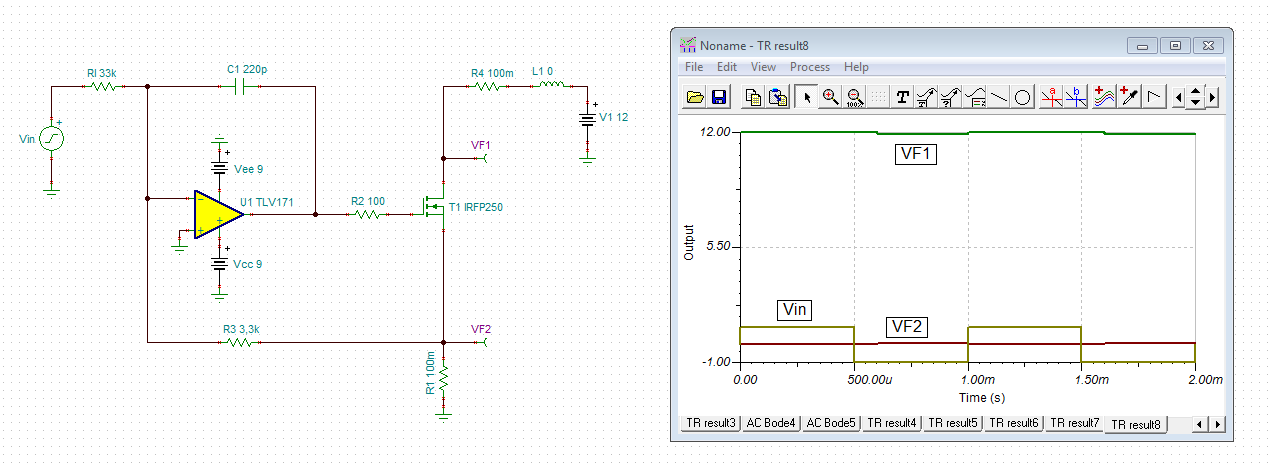
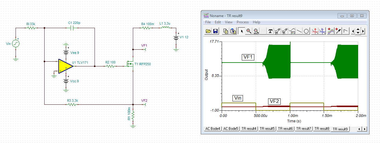
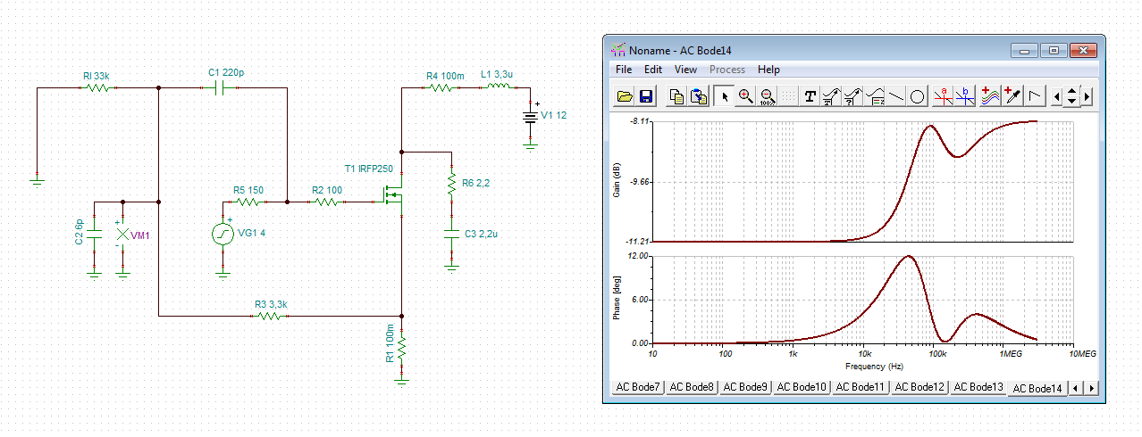
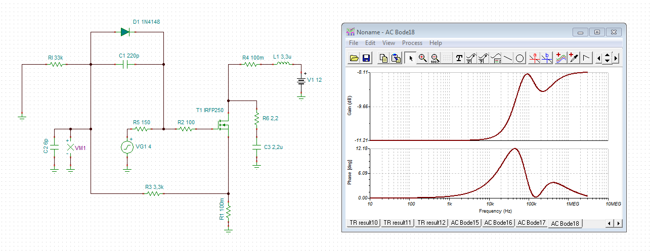
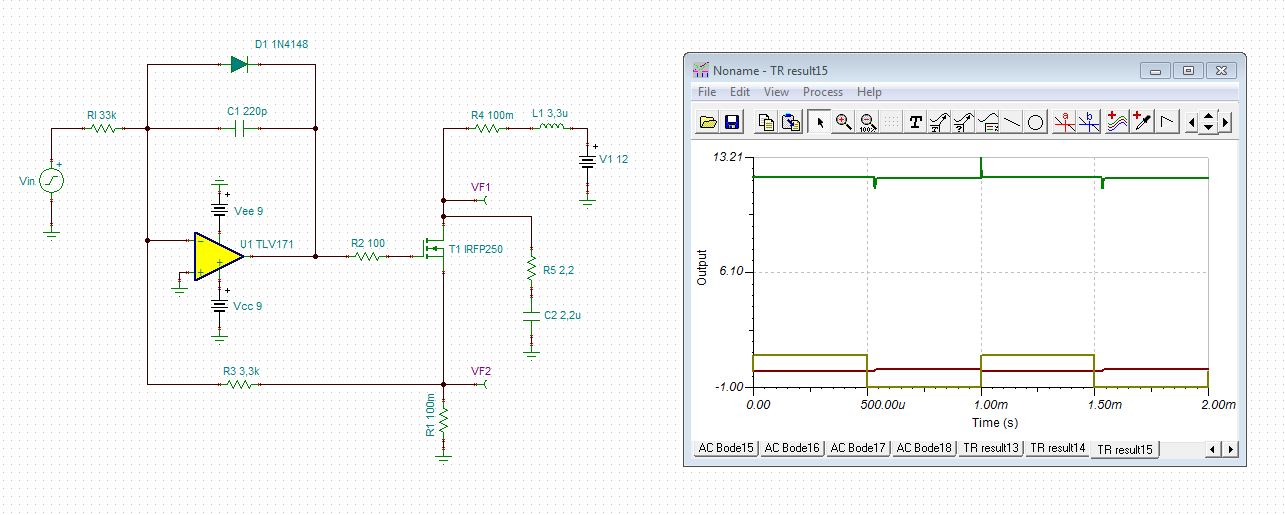
I misread the information, originally, and laid out a dual-supply circuit. Schematic attached.

Thank you, for your help.

Ts Dual TLV171_IRFP250 FGI E_Load (1).pdf

  • Hi Tom,

    the circuit looks well with your bipolar supply voltage.

    The usual input bias cancelling resistors from the +inputs of TLV171 to GND are not needed when working with the TLV171, though, because the input bias currents are ultra low.

    Have you carried out a phase stability analysis of the MOSFET driver stage?

    Kai
  • Hi Tom,

    The TLV171 can be used with a single or dual supply. When a datasheet refers to a device being single supply it typically means that the device has a common mode voltage that extends to V- (Ground when using single supply) but it does not mean that the device can't be used with dual supplies. I recommend watching our TI Precision Lab videos on input and output limitations for more information.

    As Kai mentioned I recommend doing a stability analysis on the MOSFET driver stage. Depending on the capacitance of the MOSFET its very possible that the circuit is unstable. For help doing a stability analysis on the circuit we also have some TI Precision Lab videos on Stability. I also agree with Kai that the Ib cancelling resistors are not needed.

    Thank you,

    Tim Claycomb

  • Thanks, Kia, for the good information.

    So, the +input can go straight to ground? That makes me a bit nervous, as it is not typical, IMHO... But a component saved, is a penny earned... <grin>

    As for stability analysis... Being a noob, I wanted to work with a known circuit. This one originated from Jay Diddy B, over at the EEVBlog forum... IIUC, it is supposed to be somewhat universal, as to op amp and MOSFET selections. I wanted heavier MOSFETs and other posters had suggested better op amps... I am finishing up the PCB layout. I will be able to, easily, cut and paste the driver and order a small board from OSH Park, for testing. For $5, that beats bread-boarding, on several levels...

    I only have a Tektronix 2215/60MHz oscilloscope, to look at the stability... I have heard of significant oscillation problems, as high as 200MHz, with other designs, so I may not be able to see a problem. But, I will, surely, give it a look. I do not know how to simulate the design, yet.

    For full disclosure, I posted the data sheet question, here, because I had received a comment that the TVL171 would not work, in my dual supply design. I reread the data sheet and found a glimmer of hope that it would work. I had a lot of work, in the design and I needed a definitive answer. I knew, that as for a TI product, this would be the place to get the correct answer.

    Thank you, for your help.

  • Thanks, Tim.

    I knew about powering op amps, but it slipped my mind. Thanks, for the refresher.

    I will give the videos a look... Does the MOSFET circuit design look suspicious, or was that a general comment?

    Thank you, for your help.
  • Hi Tom,

    I have done a simplified phase stability analysis and can confirm that an inductance in the load line can make the circuit oscillate, when omitting a snubber at the output.

    Without an inductive load the circuit is stable:

    But with an inductive load of 3.3µH the circuit becomes instable:

    As it can be seen in the phase response plot the oscillation will occur at about 200kHz.

    A snubber at the output cures the instability:

    One note to the simplified phase stability analysis: A gate source voltage of 4V must be set to turn-on the IRFP250 in the simulation. The correct value was found with the transient response analysis with the 1kHz square signal above.

    Finally, the plots for your circuit with the added diode:

    So, your circuit should work!

    Tom.TSC

    tom1.TSC

    Kai

  • Wow, Kia, what a gracious effort. Thank you! I will study your notes and add the snubber.

    Yes, I think I said 200MHz, but 200KHz seems more like what I remember. I should be able to see that...

    Thanks, again!!!

  • Hi Tom,

    I do not recommend using Kai's method to simulate the stability of an amplifier. While Kai's method is a simplified method the method provided in the TI Precision Lab videos only need an inductor and capacitor to simulate the same things. The reason I do not prefer Kai's method is because the output impedance of an amplifier is not always resistive (like what is shown in Kai's method). For example, the TLV171 output impedance is capacitive inductive and resistive (see figure 13 in the TLV171 datasheet) which can have negative effects on the stability of the amplifier. If the capacitive load you are driving interacts with the inductive area of the open loop output impedance the op amp will likely be unstable.

    Therefore, I highly recommend using the method shown in the TI Precision Lab videos so that the correct open loop output impedance is included in your simulation.

    Thank you,

    Tim Claycomb

  • Tim,

    the transient analysis which takes into account the complex open loop output impedance of TLV171 also shows that the circuit is stable. I show it again with the added TLV171's output signal:

    The output voltage Vo is free of any overshot and ringing. So, the erosion of phase margin due to the gate source capacitance of IRFP250 within the feedback loop of TLV171 is adequately cured by the phase lead capacitance C1.

    Tom, to see how important C1 is, I have omitted C1 in the following transient analysis:

    I have zoomed the region arround 500µs to show better the overshot and ringing. Without C1 the phase margin is heavily eroded!

    Tom, take this transient analysis to check the stability of your circuit. Just add the actual load you intend to drive, modify the input signal and run the transient analysis. If no overshot and no ringing can be seen at the output Vo, the circuit will be stable.

    Tom3.TSC

    Kai

  • Thanks, Tim and Kia. Both of you certainly have gone above and beyond the call.

    This is the thread link, should you have interest.
    www.eevblog.com/.../

    Tim, I think I may get a free shipping coupon, for marking the thread as resolved. If so, what TI op amp/MOSFET combination, would you suggest? And, is there a complete schematic, somewhere?

  • Hi Tom,

    A few high voltage op amps I would recommend are the OPA172 and the OPA192.

    I'm no expert in choosing a MOSFET for your design but you could post another E2E question to see what someone has to recommend or you can check out all our MOSFETs by going here. You can easily eliminate the number of options by using the filters on the left side of the page.

    Regarding a complete schematic, are you referencing a schematic earlier in one of your posts? Or are you just looking for any document to help in your design?

    Thank you,

    Tim Claycomb

  • Hi, Tim,

    "Or are you just looking for any document to help in your design?"

    When I started in, on the process of building an e-load, I looked around for a known DIY design, of good reputation. There did not seem to be any particular one, that folks were really raving about. That put me in the design mode.

    Working on the design has been the best way to learn the circuit. I have learned tons, on this just one project, alone. But, it does put off the building phase, which I r-e-a-l-l-y enjoy. And, there is some uncertainty, that the new design will work.

    Some manufacturers post typical usage designs, in component data sheets, and, sometimes, they offer very unique, complete projects. So, I was asking if TI had any e-load schematics, of that ilk.

    Thanks for your support!
  • Hi Tom,

    the major issue in this circuit is the gate source capacitance of MOSFET. The higher this capacitance is, the more difficult it becomes to stabilize the OPAmp. The gate source capacitance adds phase lag in the feedback loop and erodes the phase margin. A phase lead capacitance is needed to restore the phase margin, if not totally then at least to a value which allows the OPAmp to run stably. Unfortunately, this phase lead capacitance slows down the output of OPAmp and does not allow to turn-on the MOSFET ultra quickly.

    All this information can be gained from the simulation. Play with it, change the component values and look what happens. A lot can be learned from such simulations, even if they might not tell the whole truth. :-)

    There's another issue with this sort of circuit. A big MOSFET not only shows a big gate source capacitance but also a considerable drain gate capacitance which can inject load transients entering the drain terminal (ESD, inductive kick backs, etc.) directly into the output of OPAmp. So, the 100R gate resistance serves two functions: First, it prevents the MOSFET from oscillating itself and second, it limits the current into the output of OPAmp when a transient enters the drain terminal of MOSFET.

    So, it's a good idea to choose an OPAmp which has a high ESD rating. Additionally, if you plan to drive inductive loads with your circuit, I would add some protection circuitry against inductive kick backs. Also, directly at the output of OPAmp protection diodes could be added to the rails. And from each rail to signal ground a TVS could be added.

    But do not increase much the gate resistance. This will increase the phase lag in the feedback loop and will furtherly slow down your circuit. For the same reason it's not wise to choose an OPAmp which draws only very little supply current and, because of this, shows a high open loop output impedance. So, the TLV171 is not a bad choice for your circuit.

    Kai
  • Hi Tom,

    I'm not aware of any documents specific to electronic load designs but we do have designs that discuss Voltage to Current converters which is essentially what you appear to be building. Take a look at these documents on V to I converters.

    High-Side Voltage-to-Current (V-I) Converter

    Low-Side Voltage-to-Current (V-I) Converter

    Then you must verify your amplifier is stable. I recommend taking a look at "Capacitive Load Drive Using an Isolation Resistor" and watching our TI Precision Lab videos on op amp stability.

    Thank you,

    Tim Claycomb

  • Kia, this is an excellent explanation. I have copied it, to study it further. You certainly have earned your guru status. ;-)

    Tim, thank you, for the links.