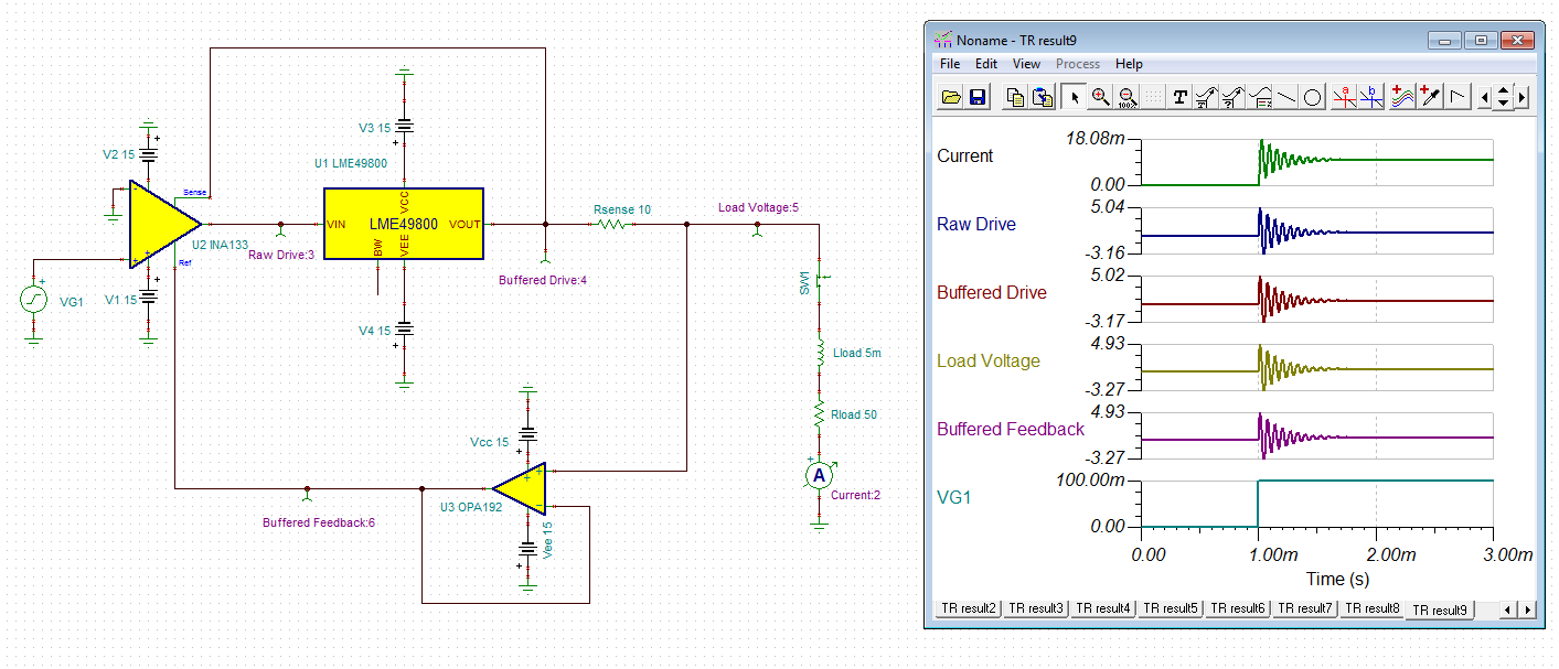
I need to construct a V -> I conversion circuit with a gain of 100mA/V and +-200mA drive capability. The frequency requirements are not high, and bandwidth of 2kHz would more than suffice. However the circuit needs to operate with a wide range of resistive & inductive loads. With an inductance range of 0 to 100mH and resistance of 0.1R to 500R (Understanding that the current will be limited at higher resistances by the +-15V supply rails)
My AC analysis is a bit rusty and I have been trying to work through the guides found here https://training.ti.com/ti-precision-labs-op-amps-stability-3 to calculate the phase margin.
However I am not quite sure the correct location to break the feedback loop at, in particular since the Howland current source also has positive feedback.
I have attached my TINA simulation.