This thread has been locked.

If you have a related question, please click the "Ask a related question" button in the top right corner. The newly created question will be automatically linked to this question.

INA148: Is INA148 suitable for our application

Part Number: INA148
Other Parts Discussed in Thread: ISO124, INA240

Hello,

Our application can be described using 2 images. 

Case 1:

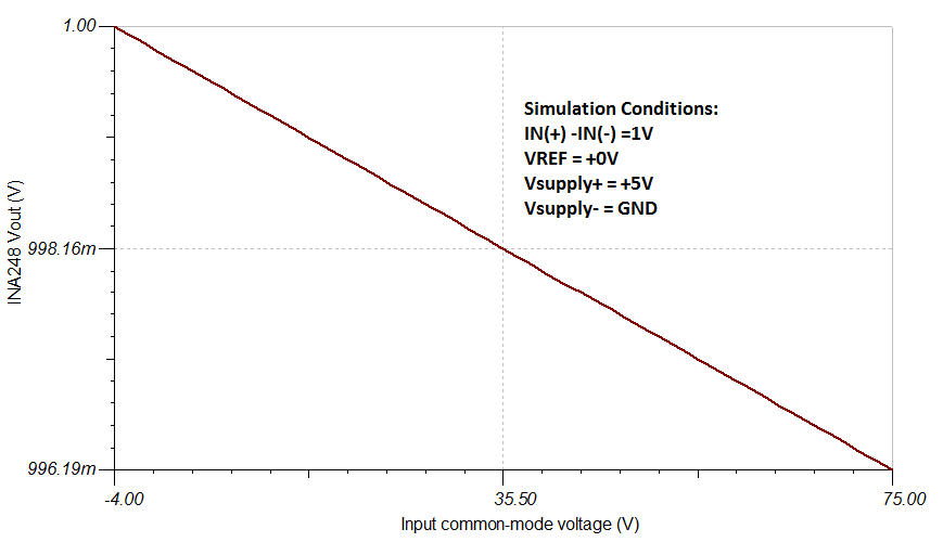
Doubt related to this case: Will the IC work as expected even if Ref = 0V. What will be the CMV range in this case, as the data sheet only gives this value of Ref=0.25V or Vs/2.To put it in short, for minimum voltage at In- will this IC work correctly with Vref = 0V. Given VIn+ is always greater than VIn-.

Case 2:

Doubt related to this case: 

1. Will the IC work as expected even if there is no common ground connection with the sensed circuit as shown(Expecting an issue with return path for bias current).

2. We are thinking of using this high common voltage IC because we think as the ground will be different in the second case, the IC might get damaged due to high common voltage which might appear at the input due to difference in the two ground voltages. Measuring the voltage isn't critical in the second case, we just want to ensure that the IC doesn't get damaged. Do you think this is an overkill and we should go for normal low common voltage differential amplifier?

Note - 60 V is the maximum capacitor voltage in our application and corresponding In+, In- voltages wrt capacitor ground is 2.5V, 1V.

  • Hi Shyama,

    As you have mentioned, the datasheet specifies the common-mode voltage range for the condition where (VIN+) - (VIN-) =0V  (differential input voltage is 0V) and VREF=0.25V, and unipolar +5V.   This is to keep the device in the linear region.  One thing to keep in mind is that the INA148 output stage is limited by the supply rails, and in case 1, the output swing is limited between 250mV and +4V.  Since the output is a function of the input differential plus the voltage at the reference pin (in this case 0V), the device will only remain in linear operation for the case the differential input signal exceeds positive +250mV+(INA offset) or Vin > +255mV.

    Attached is a TINA simulation of the output voltage as the common-mode voltage range changes.  For the case where V+=5V, V-=0V, VREF=0 and the input voltage is fixed, (VIN+) – (VIN-) = 1V, the device can work with a common-mode voltage of -4V to +75V.  Also, your schematic of case (1), where the GND pins are connected, suggests the common-mode voltage and differential voltage will always remain positive.    

    You are correct, on case (2), the difference of the INA148 device GND and the GND of the input signal must not exceed the common-mode voltage specification or the device will be outside of its linear region.  In the case of INA248 with the +5V unipolar supply and VREF=0V, the GND voltage difference cannot exceed approximately -4V to +75V.  If you expect the GND difference will be greater than this voltage, you could set REF=2.5V to extend the range, to -47.5V to +32.5V with +5 unipolar supply, or use ±5V bipolar supplies to extend the common-mode range to -100V to +80V with VREF=GND.  If the common-mode exceeds ±200V, damage will occur to the INA148.

    If you expect the GND difference to exceed these common-mode voltages, you could consider an isolation amplifier, for example ISO124.

    Thanks and Regards,

    Luis

    TINA simulation file:

    INA148_commonmode.TSC

    INA148 TINA simulation Result:

  • Hi Luis,

    Thank you so much. But you missed one thing. We asked if the IC will work properly even if the ground of input signal and differential amplifier are not the same? (Assuming the common mode voltage is within the permissible limits) I understand the IC will not get damaged but will it be able to give correct output voltage, as there is no return path for any bias current back into the sensed circuit. I had mentioned this in the first part of the second case. Please see to it.

    I am not good at Analog Electronics, any help would be appreciated. :)
  • Hi Shyama,

    it's not necessary to create a path for the input bias currents outside of INA148. The inbut bias currents can flow internally of INA148. Otherwise the AC-coupled difference amplifier shown in figure 5 could not work.

    But please read very carefully section "input impedance" of datasheet.

    Kai
  • Hello Kai,

    Does that mean, when it comes to bias current, INA148 is completely different from INA240? I am saying this because Mr. Guang said that the INA240 requires a DC bias current from the sense circuit in the following conversation:

    e2e.ti.com/.../735065
  • Hi Shyama,

    yes, I think the INA240 is different from the INA148, because it contains an additional "internal bias network" scheme at the inputs. See also section 9.1.1 of datasheet.

    Kai