A related question is a question created from another question. When the related question is created, it will be automatically linked to the original question.
If you have a related question, please click the "Ask a related question" button in the top right corner. The newly created question will be automatically linked to this question.
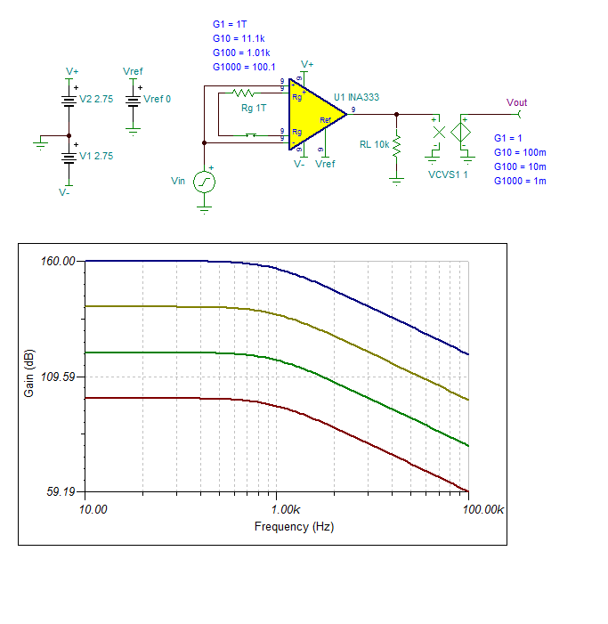
To test the CMRR of an instrumentation amplifier, you apply an AC test signal common to both of its inputs and measure the output. To refer back to the input, the output must be divided by INA gain. For example, if the INA is set up for G=1000 you must divide the output by 1000, and so on. I've attached a test circuit you can use for reference.
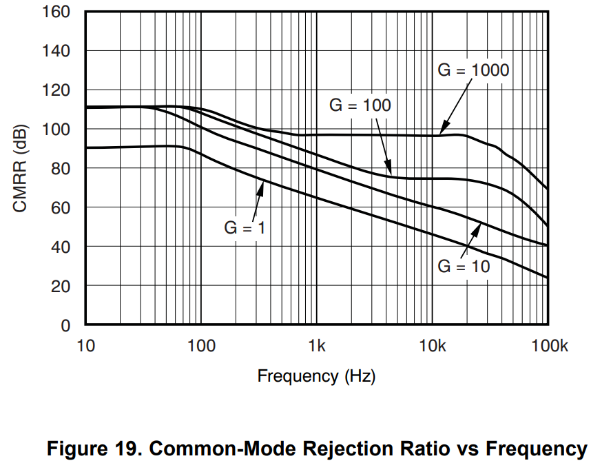
In an attempt to replicate the CMRR curve from the datasheet of the device, page 10, I set Vs+ to 5V, Vref to midsupply (2.5V) and Vs- to ground.
Simulating your reference circuit with above conditions for Gain of 1000, the CMRR curves give 150dB at around 10 Hz whereas the datasheet predicts this around 110dB. Am I doing something wrong here?
What is the purpose of in series switch with gain setting resistor ?
the common mode rejection given in the datasheet is specified for a common mode voltage which is going much closer to the rails than what is assumed in your simulation. This can degrade the common mode rejection.
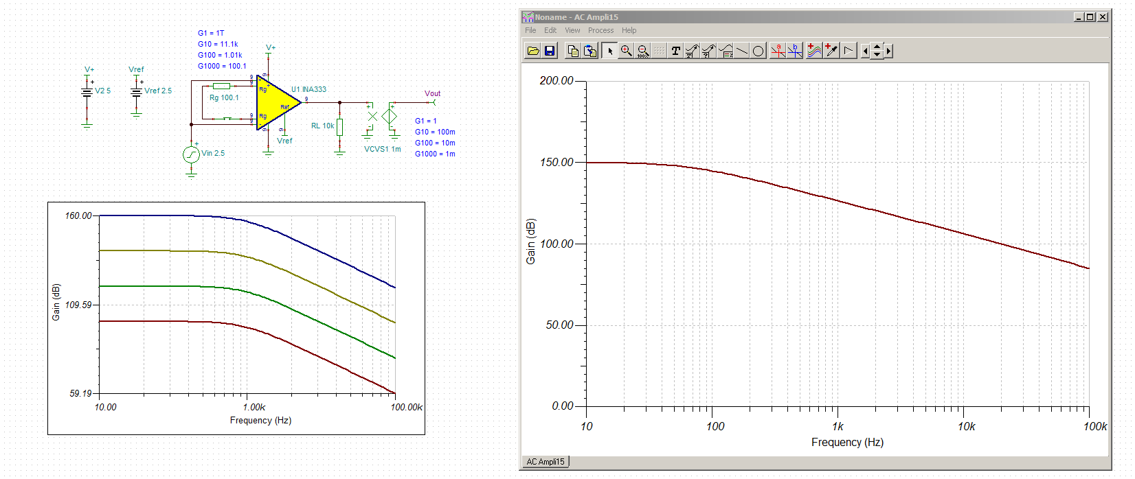
There is currently a limitation in our INA SPICE model architecture related to CMRR. While the input-referred CMRR of an INA will eventually hit some maximum at high gain, as shown by Figure 19 in the INA333 data sheet, the model's will keep getting better and better as gain increases. That's the source of the discrepancy.
The purpose of the switch in series with the gain setting resistor is so that you can open the circuit for G=1. You can also achieve G=1 by keeping the switch closed and setting RG to a very high value like 1T.
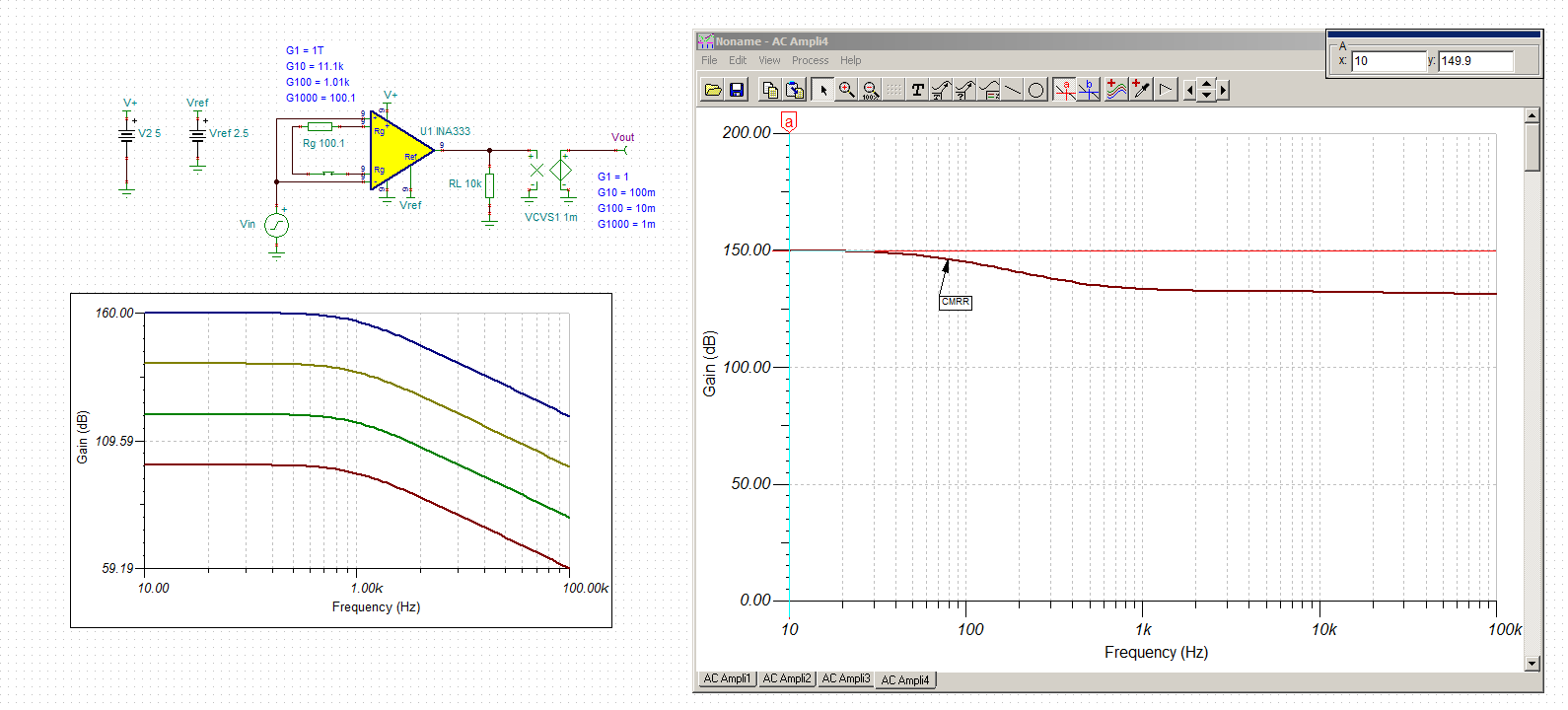
As Kai mentioned, the Vcm of the circuit is also a concern. In the split-supply configuration I attached, Vcm = 0V which is mid-supply. If you change to a single-supply configuration where Vs=+5V, make sure to adjust your Vcm to +2.5V as well as your Vref.
Thanks for the explanation. I have changed Vin(common mode voltage) to +2.5V. The AC CMRR response remained unchanged.
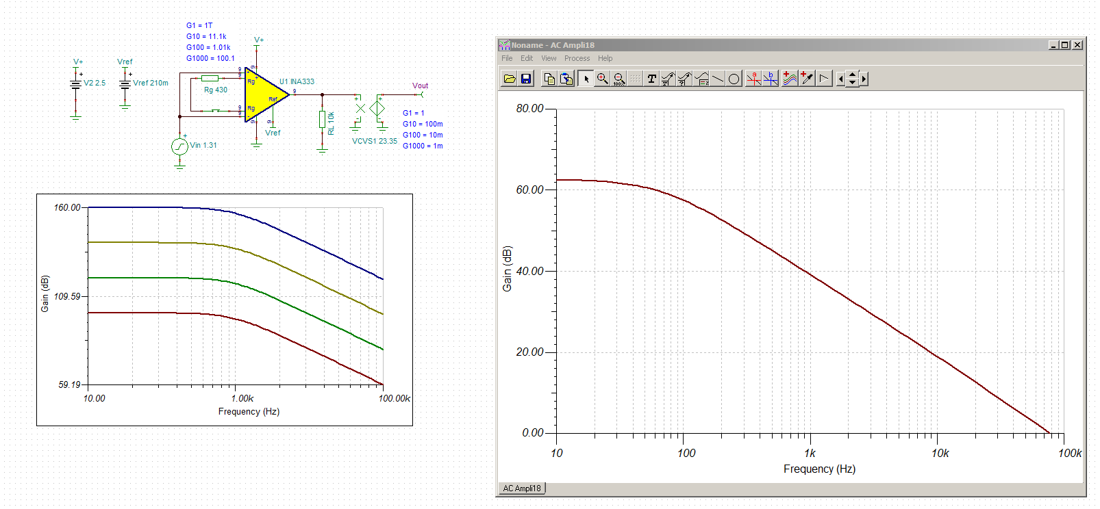
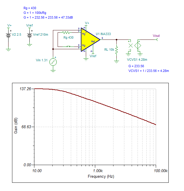
In my actual application, I have single supply configuration with Vref set to +210mV, and Vs = +2.5V with Rg set to 430 ohms representing Gain of 233.55(V/V).
The DC common mode voltage at the inputs is around 1.314V.
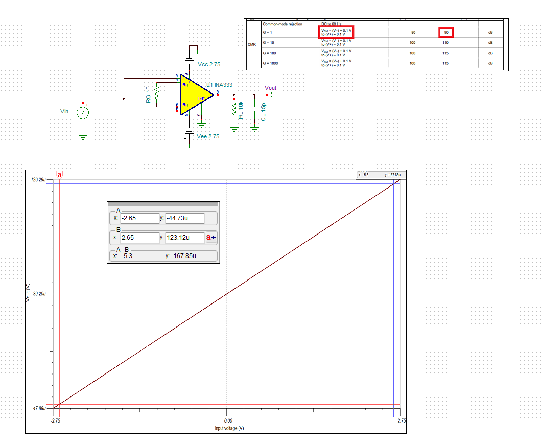
Provided there are limitations in the TINA model for INA333 like you have mentioned, is the representation of CMRR response below valid ?
Thank you for clarifying your application specifics. There are no problems with your power supply, Vcm, or Vref values.
Regarding the CMRR result, per Figure 19 of the data sheet the maximum CMRR of the INA333 is 115dB, which occurs at gains of 100V/V or greater. Since you are operating at a gain of 233.55V/V the CMRR will be 115dB.
By the way, when testing CMRR in simulation with G=233.55 you should set VCVS1 = 1 / 233.55 = 4.28m to refer the result back to the input. With our model we get a result of 137.26dB which is better than the real world.
We are working on several major fixes to our INA SPICE model architecture which will address this and other limitations, so I apologize for the inconvenience. Please let us know any other questions or concerns that you may have regarding your INA333 design and we'll be happy to help.
Thank you for suggestion on VCVS1. It makes sense.
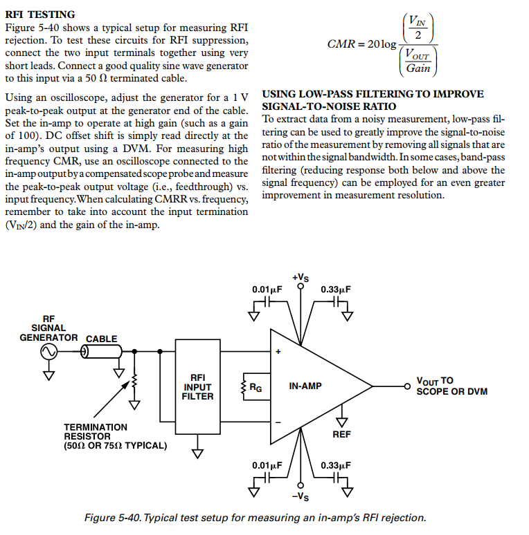
I was wondering if its possible to do a bench measurement of the CMRR with a function generator and oscilloscope. Where can I find guidelines to do so ?
I also have the INAEVM-MSOP8 evaluation board so I can use that too if necessary.
Such a measurement may be 'simple' perhaps but 'simple' isn't the answer I was looking for. I was expecting to be pointed out to a specific TI application note. Enough time has been wasted to make INA333 spice model to produce sensible results.
Analog Devices on the other hand have published better guidelines for their devices. I recommend TI do the same or at least provide better than 'simple' guidance.
Sorry for the delayed reply. We don't have any existing app note or other documentation that I'm aware with more specific guidelines for measuring INA CMRR. However, I have reached out to our characterization team to see what setup they use and I will reply when I have more information.
I got some tips from our characterization team. To measure CMRR vs. frequency, Kai's suggestion is correct in that you make the measurement the same way as shown in simulation: tie both inputs together, sweep a small input signal over frequency, measure the output transfer function, and divide by the INA gain to refer the result back to the input.
To get good results in the mid-to-high frequency range, make sure to do the following:
Keep the PCB traces on the INA input pins as well-matched as possible so that their impedances are the same. Be wary of any parasitic capacitance or inductance caused by PCB layout.
Solder the two input pins of the INA together to make sure there are no parasitics between them.
Keep the PCB traces on the INA RG pins well-matched, and prevent any parasitic capacitance there by removing PCB copper areas on adjacent layers and nearby on the same layer. Capacitance at either RG pin can create differential poles in the output stage transfer function which degrade CMRR.
Measuring DC CMRR is much more involved. It requires a specialized, high-precision test setup, measurement techniques, and data processing in order to get accurate results.