Because of the holidays, TI E2E™ design support forum responses will be delayed from Dec. 25 through Jan. 2. Thank you for your patience.

This thread has been locked.

If you have a related question, please click the "Ask a related question" button in the top right corner. The newly created question will be automatically linked to this question.

OP07C: About the size of feedback capacitor in differential operational amplifier circuit

Part Number: OP07C
Other Parts Discussed in Thread: OP07

Hi kai!

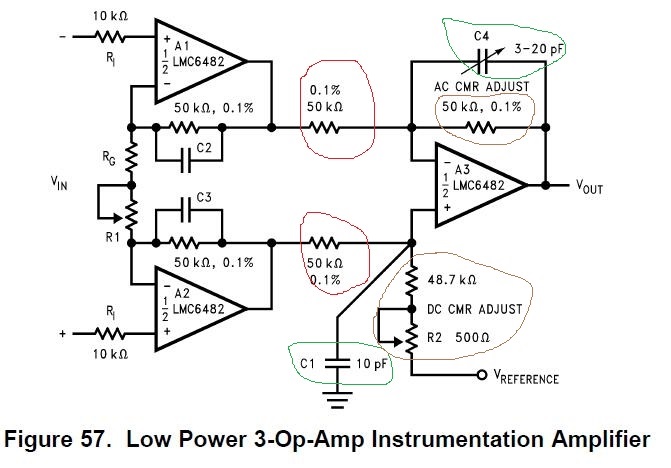
As shown in the following figure:

The red marked resistor and the brown mark resistor constitute the differential circuit of 1:1.The capacitance of C1 and C4 constitutes compensation capacitance.As you can see from the diagram, the value of capacitance is usually 0~20P?The resistance of red and brown marks must be equal?If I use a red mark with a resistance of 120 K (0.1%) and a brown mark with a resistance of 75 K (0.1%), how can I determine my compensation capacitance?In addition, when I add a compensation capacitor to the circuit, how do I verify that the capacitance has played a role? Can we see the change of output waveform with oscilloscope?Thank you!

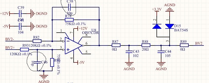
How should C38 and C46 be selected in the above image?

  • Hi Jin,

    for very high common mode rejection the 120k resistors (R82, R93) must be identical and the 75k resistors (R82, R?) must identical. And the left sides of R82 and R93 must be connected to drivers with very low source impedances.

    The capacitances C38 and C46 must be identical as well. But due to unavoidable stray capacitances, which can differ a bit for the +input and the -input of OP07, best results might be obtained with slightly different component values for C38 and C46. That's why C4 is made adjustable.

    Last but not least, you must not forget that the OP07 itself has a limited common mode rejection.

    It's very simple to check the quality of common mode rejection: Drive both inputs with an identical sine wave and observe the output of OP07. The common mode rejection is optimized when the output signal is minimum. You can take a 100Hz sine wave for the DC common mode rejection and a 10kHz sine wave for the AC common mode rejection. That's how it's done for an audio application. But there are also other methods, adjusting for optimum settling time with a square wave. e.g. It depends on your application.  

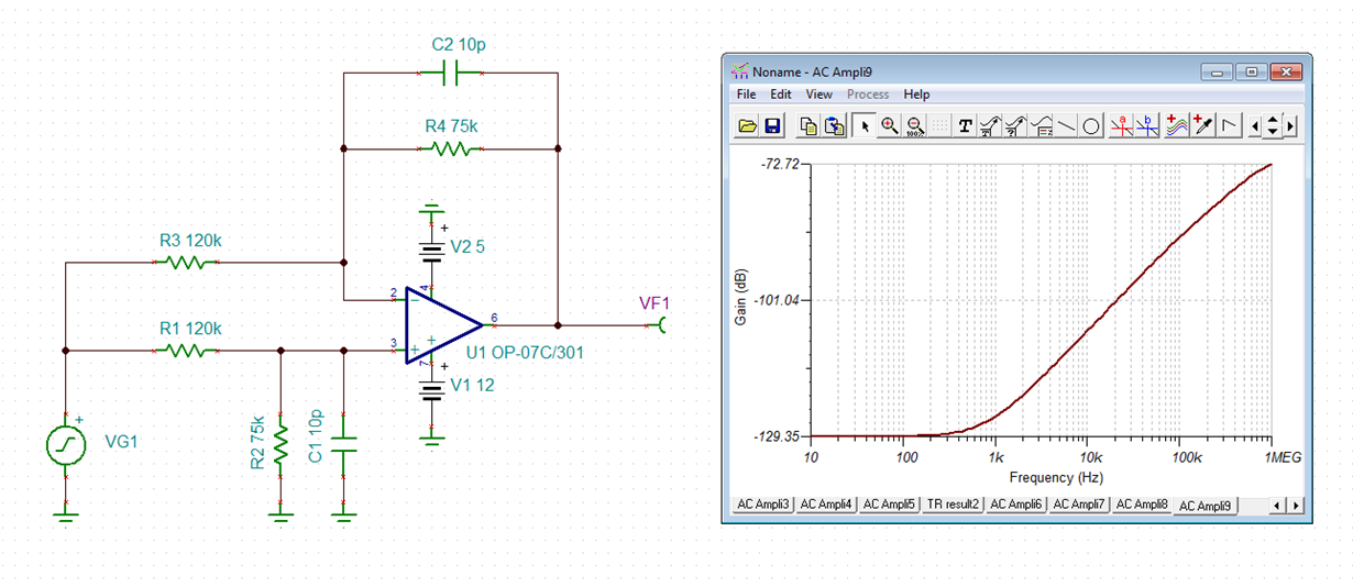
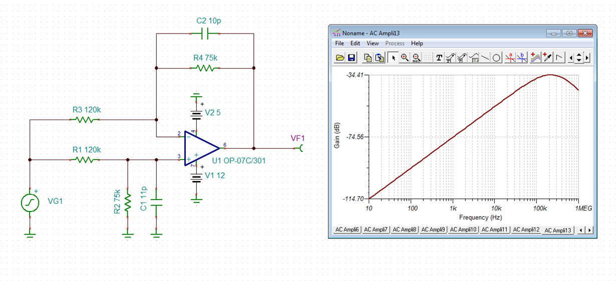
    Here are a few simulations. First the "ideal" situation when all the component values are identical:

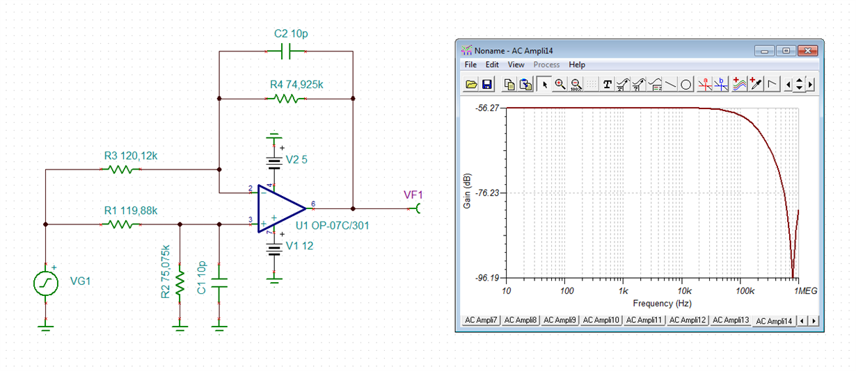
    Then the case when all resistors show 0.1% production tolerances (worst case):

    You can see that the common mode rejection at lower frequencies heavily breaks down. So, for achieving very high common mode rejection the use of resistors of even less than 0.1% production tolerances can make sense.

    Finally the case when the capacitances show a mismatch:

    jin.TSC

    10pF capacitances in the above difference amplifier were chosen to get a maximum bandwidth. But there's no need to always take 10pF capacitances. You can use higher values as well. It depends on your application.

    The best results can be obtained when using an instrumentation amplifier (INA series) where all these components are integrated on the same chip. This gives the best match of components, the least drifts (long term, temperature) and by this the best common mode rejection.

    Kai

  • Thanks very much ! kai !

    I understand INA amplifier.We use INA amplifiers on our products.But taking into account the cost and market positioning of the product being designed. So do not use INA, because INA price is higher.The output curve of the TINA simulation above can be interpreted as the curve of CMRR?

  • Hi Jin,

    concretely spoken the curve is the ratio of output signal "VF1" to input signal "VG1" expressed in "dB". It can be interpreted as the CMRR of the whole difference amplifier circuit.

    Kai
  • Jin

    We haven't heard back from you so we assume this answered your questions. If you need more assistance just post another reply below.

    Thanks
    Dennis