This thread has been locked.

If you have a related question, please click the "Ask a related question" button in the top right corner. The newly created question will be automatically linked to this question.

OPA454: difference amplifier application output error

Part Number: OPA454
Other Parts Discussed in Thread: LM741, TINA-TI, UA741

Hello,

I have a question about difference amplifier application with opa454. 

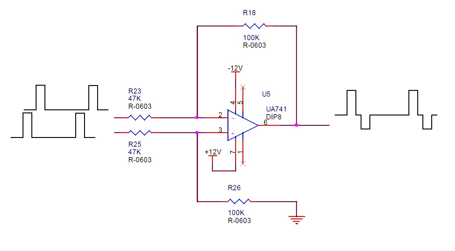
V+ = +12V, V- = -12V, IN+ = +5V and IN- = 0V or  IN+ = 0V and IN- = +5V , but output is strange. as attached

Q1: can set up float to the E/D, E/D Com and status_flag pin ?

Q2: the output pin = +12V and -7V pulse wave is correct?

Q3: When connect to load(50K resistor to ground), the output pin = +12V and -1V pulse wave is correct?

Thanks A lot,

  • Hi Peter,

    what are you using, the LM741 or OPA454??

    Why not running a simulation with the "OPA454 TINA-TI reference design", which you will find here?

    www.ti.com/.../toolssoftware

    Kai

  • Hello Peter,

    Q1: can set up float to the E/D, E/D Com and status_flag pin ?

    The E/D pin can float and the OPA454 will be enabled. See datasheet section 9.3.6, ENABLE and E/D Com. E/D Com must be biased with a voltage of (V–) minimum, to (V+) – 5 V. The status flag can float.

    Q2: the output pin = +12V and -7V pulse wave is correct?

    When the +5 V pulse is applied to the R25, R26 divider at the non-inverting input the output should be a +10.6 V pulse at the output. Then, when the +5 V pulse is applied through the inverting input path via R23 the output should be a -10.6 V pulse.

    Be sure that the selected op amp input common-mode and output swing voltage ranges are capable handling these levels. Note that for the OPA454 the Common-mode voltage range for linear operation is (V–) + 2.5 to (V+) – 2.5 V, and the Voltage output swing from rail is (V–) + 1 (V+) – 1 V, for RL = 49 kΩ, AOL ≥ 100 dB, IO = 1 mA and Vs +/-50 V. They may be somewhat different with the +/-12 V supplies. The OPA454 is optimized for +/-50 V operation.

    Q3: When connect to load(50K resistor to ground), the output pin = +12V and -1V pulse wave is correct?

    For the OPA454 I would expect to see the +10.6 V and -10.6 V pulse amplitudes.

    Be sure you have the OPA454 underside PowerPad soldered to a PC board pad connected to the V- voltage level.

    Regards, Thomas
    Precision Amplifiers Applications Engineering
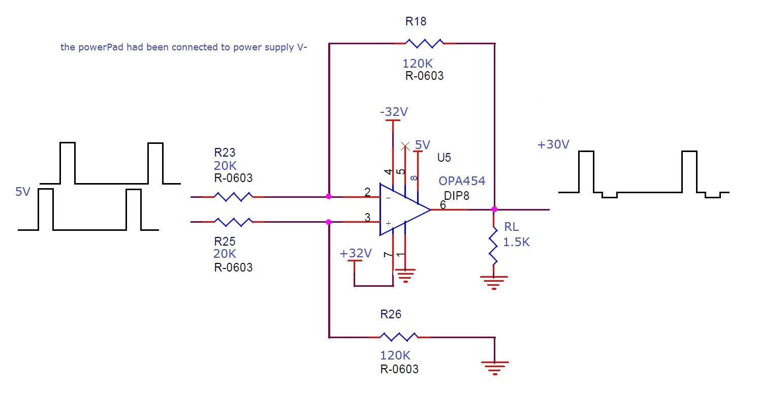
  • I had modified my circuit diagram and test board as attatch.

    Q1: My old circuit board could output +/- 12v pulse with UA741. The new circuit board that i would expect to see the +/- 30v pulse amplitudes with OPA454. But the result is +30v and -1v pulse amplitudes output. Why?

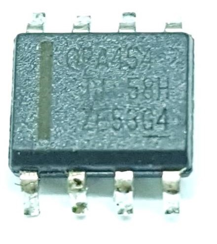
    Q2: Another photo is OPA454 chip. I bought it from the internet. is that Original equipment manufacturer?

    Q3: Is there any alternative?

    Please give me some suggestion or idea.

    Regards, Peter

  • Hi Peter,

    hmm, should work.

    The input signals, do they have the same GND reference as the GND of OPA454 circuit?

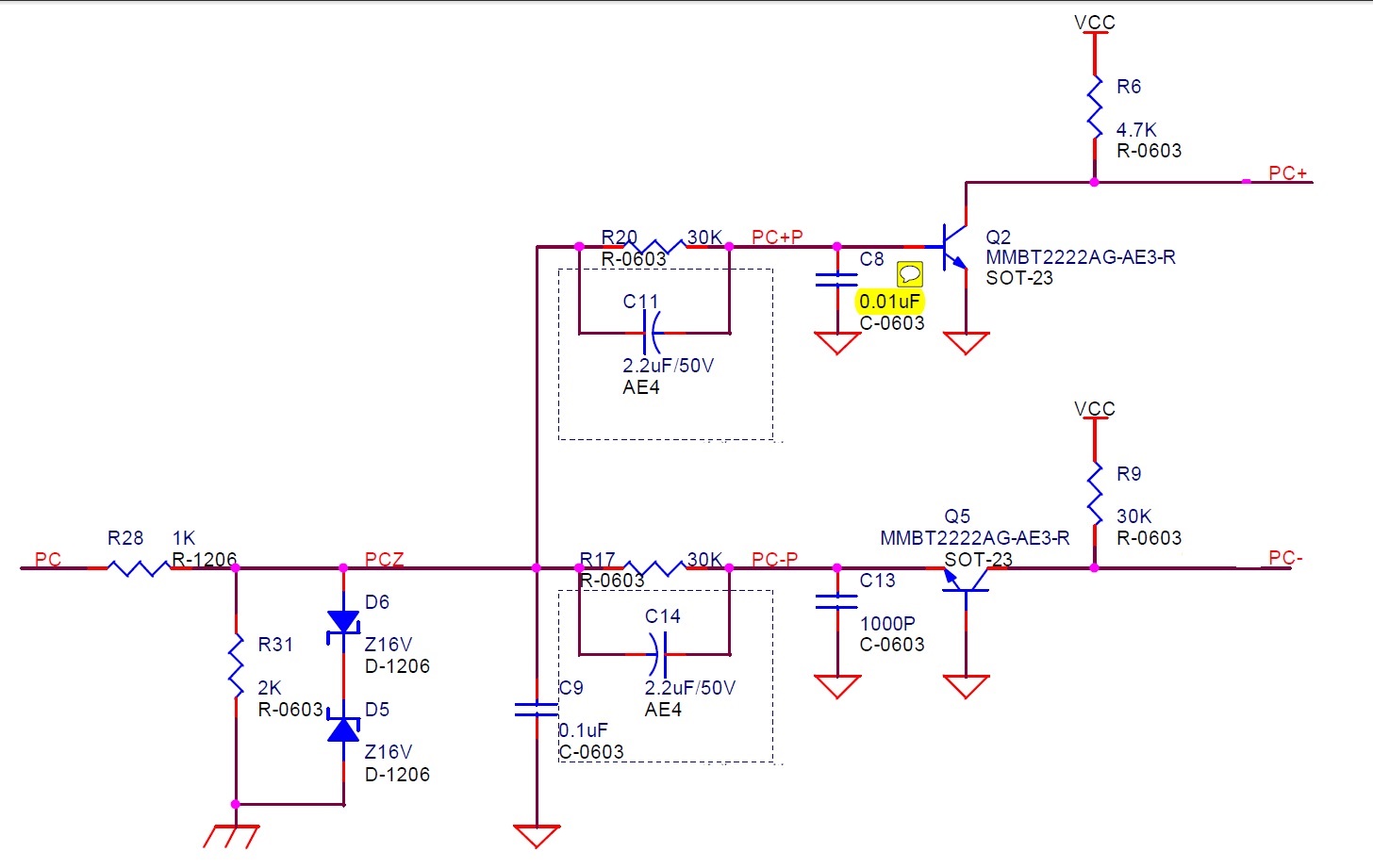
    Is the output of OPA454 connected to anything? Maybe to an input which's circuitry is powered by a single supply voltage, so that the negative going output amplitude of OPA454 could be clamped by any pn-junctions?

    Can you show a scope plot of the input signals and output signals?

    By the way, do never buy a chip from an unkown source in the internet, but only from an authorized TI distributor!!

    Kai

  • Hi Peter,

    I agree with Kai's assessments; the circuit should work as expected with the OPA454. I suspect either there is circuit wiring error, the OPA454 output is damaged, or the OPA454 device used really isn't a real OPA454. If you have another OPA454 I would try it in the circuit and see if you get the same result. Do add power supply bypass capacitors to the op amp V+ and V- pins to ground as a standard engineering practice.

    Unfortunately, because of product counterfeiters pirating any lot code information I might provide I am not permitted to verify the authenticity of the OPA454 device you show in the image. Just be sure you obtain an OPA454 directly from TI, or one of its authorized distributors.

    Regards, Thomas
    Precision Amplifiers Applications Engineering
  • Hi Kai,

    ans1:Yes, The input signals(5v pulse ) from mcu's IO pin. They have the same GND reference as the GEN of OPA454 circuit.

    ans2:The power supply has add bypass capacitors to the op amp V+ and V- pins to ground.

    ans3:The output signal of OPA454 is connected to another circuit board as attatch. I expect a +5V signal to appear on PC+ and PC-

    Regards, Peter

  • Hi Peter,

    disconnect the above circuitry from the output of OPA454. Is the OPA454 working now?

    The input signals come from a microcontroller's IO pins? Are these true push-pull outputs or quasi-bidirectional IO pins from a 80C51 type microcontroller which need pull-up resistors?

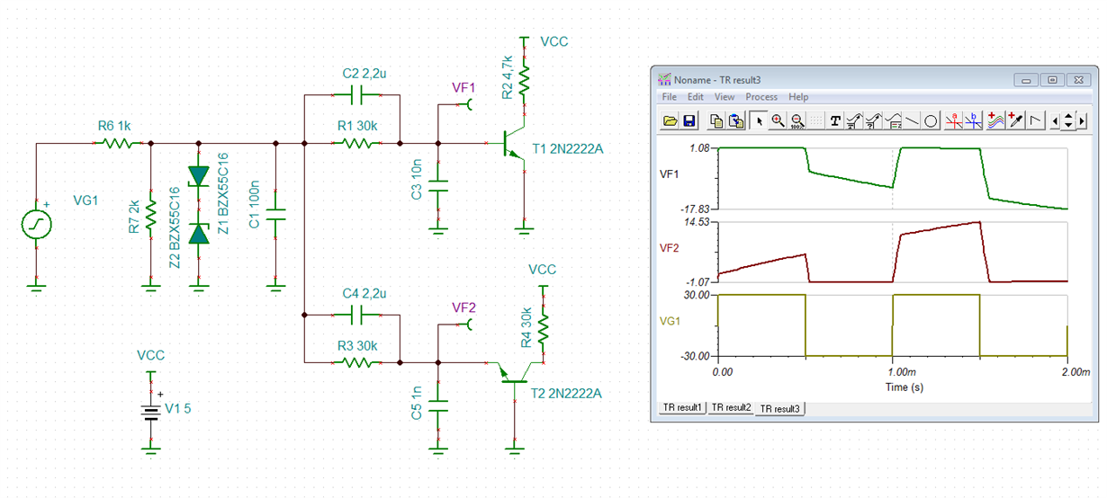
    By the way, the circuitry arround Q2 and Q5 will not work properly, because you violate the maximum reverse base emitter voltage!!

    peter.TSC

    If a transistor's maximum base emitter reverse voltage is exceeded, the base emitter junction behaves like a zener diode, as discussed here:

    www.nutsvolts.com/.../bipolar_transistor_cookbook_part_1

    Kai

  • The event that the OPA454 is unable to output a negative wave has been confirmed. Only 2 of the 10 I bought from the Internet will normally output a negative wave, and the others are not normal.
    Thank you very much for your help.