This thread has been locked.

If you have a related question, please click the "Ask a related question" button in the top right corner. The newly created question will be automatically linked to this question.

THS3061: Please tell me if small portion of my PCB layout and routing is right

Part Number: THS3061


Hi TI expert,

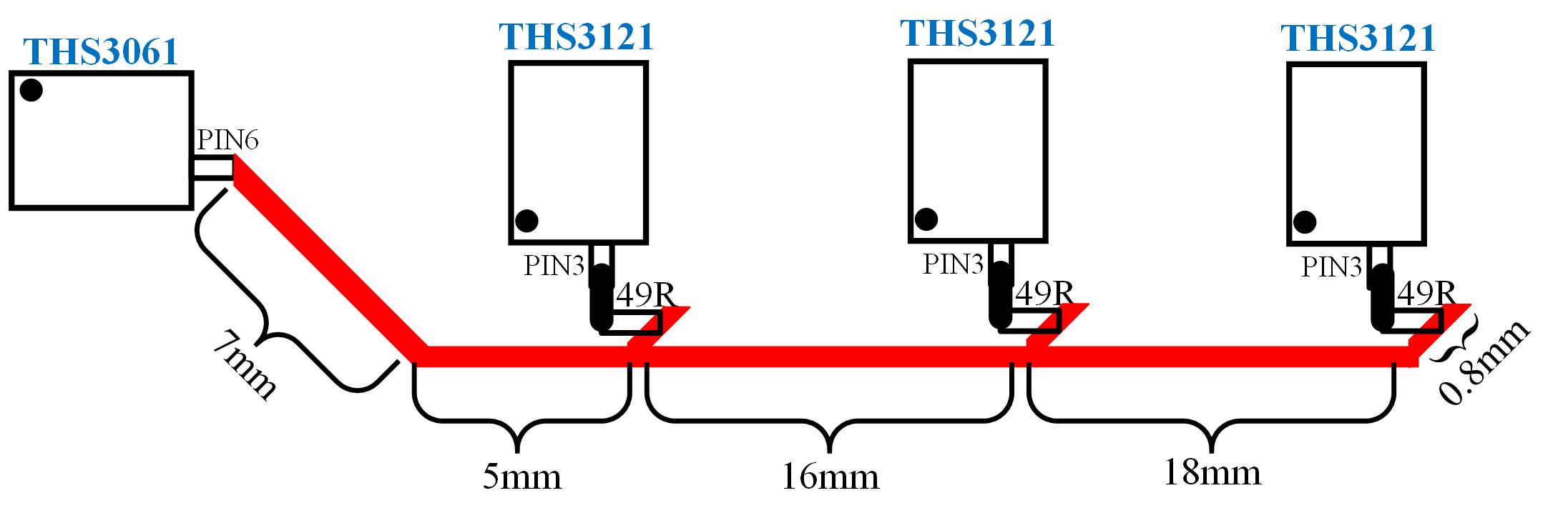
I've finished my circuit design and PCB layout, routing with your help. Red lines in Fig1 is what I'm not sure about. I've done the PCB routing and layout work as shown in Fig2, also red lines.

THS3061's output voltage may reach 400V/us. The routing trace lengths are all marked in Fig2, with track width 20mil. The power and ground plane's copper under the red tracks have all been removed. Can you tell me if Fig2 is right for such high slew rate?
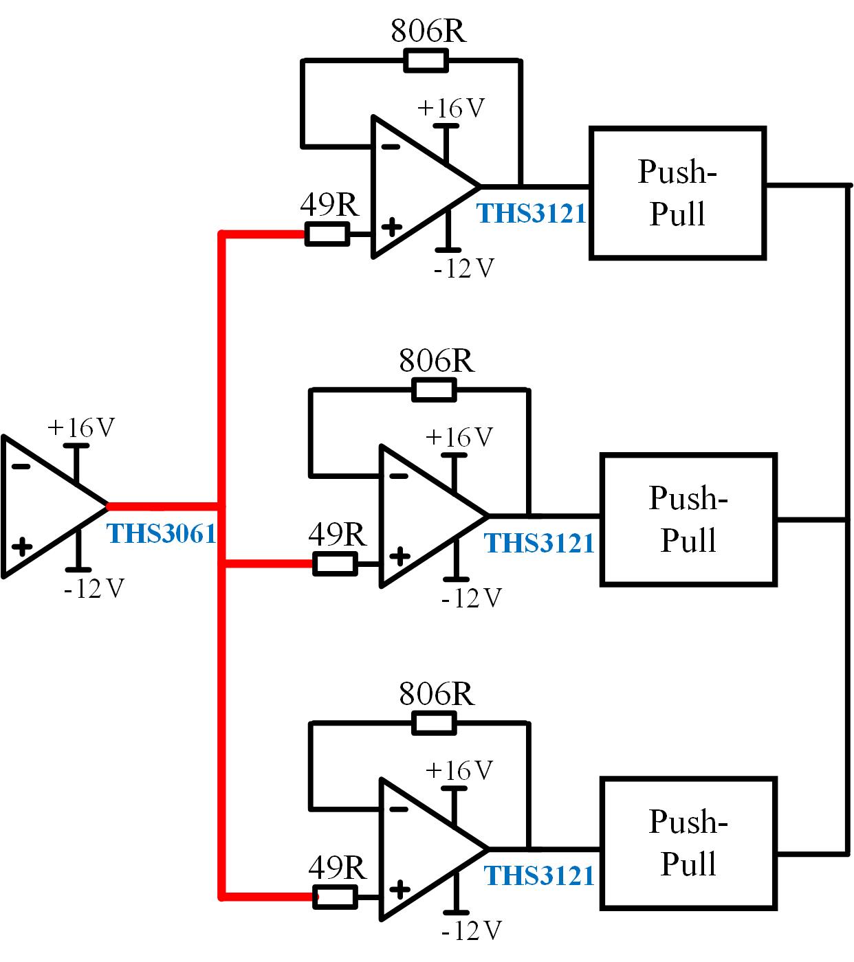
Fig1

Regards

Yatao

  • Hi Yatao,

    in any case I would place a resistor directly at the output of driving THS3061. This is a must with HF-OPAmps. I would use a 10...49R resistor.

    Then, it's better to have a ground plane under the signal line, otherwise undefined stray capacitance is charged when the output slews. By this you would force ground return currents to flow across undefined current paths full of complex impedances. This can destabilize the circuit. So, wire the signal trace as microstrip line over the ground plane.

    The usual way to connect HF-OPAmps outputs to HF-OPAmp inputs is the use of microstrip technique. For this you need a microstrip line of a certain characteristic impedance (50R...75R), a series termination resistor of same impedance at the output and a parallel termination resistor of same impedance at the farest input. Unfortunately, this would mean a signal dividing by a factor of "2". With a bit luck (if your signal trace is not too long and/or if your signal bandwidth is not too high) the signal diving can be avoided. So, I would try to reduce the signal trace length from the output of driving THS3061 to the inputs of receiving THS3061.

    To resume, route a ground plane under the signal trace, put a 10...49R resistor directly at the output of driving THS3061 and keep the signal trace length to a minimum.

    Kai
  • Hi Kai,
    U R very professional.
    My PCB has 4 layers. The signal trace of my concern is on toplayer, under which is power plane. Ground plane and bottomlayer are on 3rd and 4th layer.
    If I remove power plane's copper under the signal trace and leave ground plane intact, will this be OK? Or, I have to switch power and ground plane's position and put ground plane right under toplayer?
    As for microstrip technique, I know it just means to select the proper trace width. However, I don't know exactly how to do it. Can you provide me some easy-to-implement materials or examples?

    Regards
    yatao
  • Hi Yatao,

    in less critical applications the power plane can eventually be used for the microstrip line, provided the supply voltage is properly decoupled at each chip. But I would not recommend this!

    Usually it's not wise to have the power plane routed in the second layer in a HF-circuit. This can cause stability issues. It's better to route a ground plane in the second layer. Keep it solid and remove the copper only at those places where the datasheet of HF-OPAmp demands it.

    A microstrip line (being routed in the top layer) has to be embedded into a ground plane on the top layer and has to be routed over another ground plane beneath. Important parameters are the trace width, the distance to the ground plane within the top layer and the distance to the ground plane beneath. There are lots of microstrip calculators in the www which will help you to find the proper parameters.

    Use lots of vias next to the microstrip line to connect the individual ground planes to each other.

    Kai

  • Hi Kai
    Thx!
    Finally, can you provide me some PCB examples that use this microstrip technology? And can you please find a calculator for me?

    Regards
    Yatao
  • Hi Yatao,

    Paul has written a very nice post recently:

    e2e.ti.com/.../2789643

    There are layout examples and much more.

    And here's a microstrip calculator:

    chemandy.com/.../coplanar-waveguide-with-ground-calculator.htm

    Kai
  • Hi Kai,

    Thx.

    Paul explained  the detailed principle behind microstrip technology, and you give me a calculator. But I'm still not sure whether I understand you well. So, can you offer me a PCB project file that uses microstrip technology?

    And, just to confirm, you say " series termination resistor of same impedance at the output and a parallel termination resistor of same impedance at the farest input". The resistor's positions in Fig1 and Fig2, which is correct?

    Fig1

    Regards

    Yatao

  • Hi Yatao,

    this PDF is what Paul suggested you to have a look into:

    Please go to page 34. There you will find an example layout.

    Beside this, TI has tons of EVMs for their HF OPAmps. Have a look into them.

    To your figures:

    The second figure is wrong. Try the first figure.

    The suggestion with the "farest input" was meant in conjunction with this scheme:

    e2e.ti.com/.../3618.Fig2.jpg

    Kai

  • Hi Kai,
    Thx!

    Regards
    Yatao