Other Parts Discussed in Thread: TINA-TI, INA122
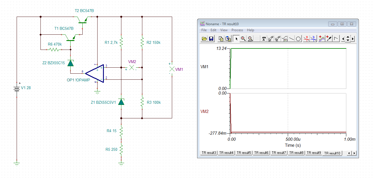
In what condition the inverting and non inverting inputs are not equal in negative feedback op amp ? I am making a simple voltage regulator . I have set my non-inverting input to 5V, thru a zener. My inverting input is fed back thru a Darlington pair and a voltage divider. I measured voltage between inverting and non inverting to be 800 mV !! Shouldnt the difference be a few mV max ? Thanks
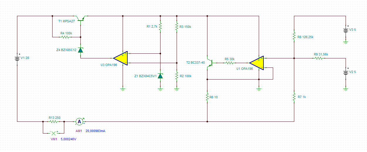
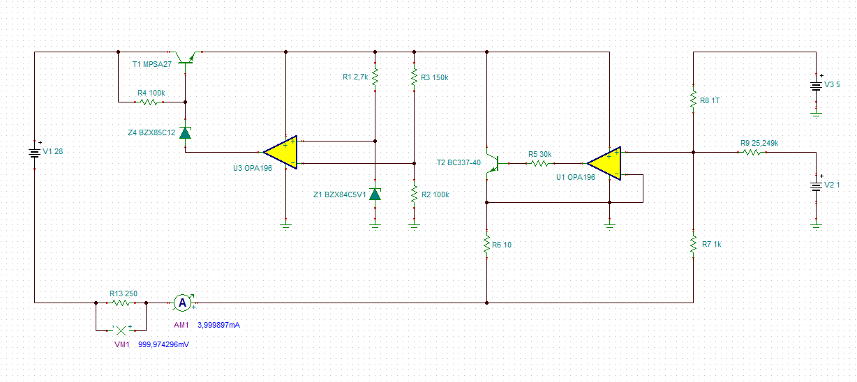
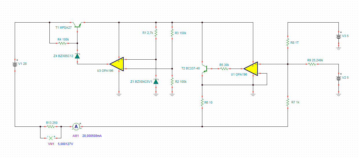
The Op Amp that I am using in the circuit is: TL35072P. Thanks