This thread has been locked.

If you have a related question, please click the "Ask a related question" button in the top right corner. The newly created question will be automatically linked to this question.

INA180: Output unstable at high frequency Load transient

Part Number: INA180
Other Parts Discussed in Thread: OPA192

Hi

Our customer is using our INA180 as current sense at server PSU. The common mode voltage is 12V.  Power supply is 16V-GND;So far we found the static and dynamic issue at test:

1. Static error:    The INA180 output will go to MCU A/D port;
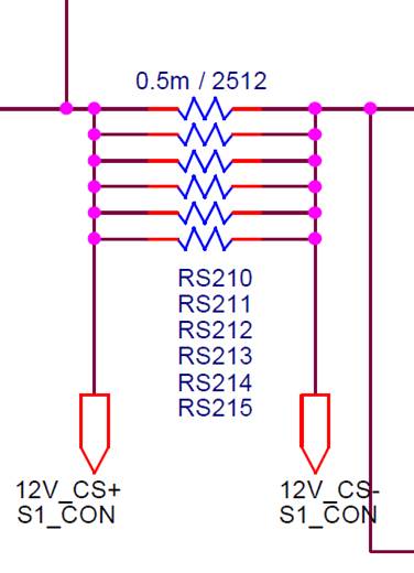
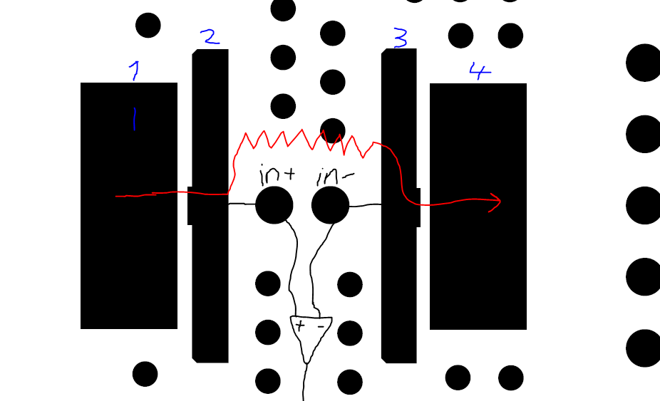
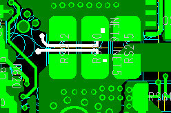
Kelvin type layout:

But we found the static output is below:

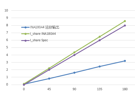
There is a little bit tolerance between I_share INA180A4(real value) and I_share Spec(ideal value). I just recommended our customer Calibrate and correct by using the software. Do you have any suggestion about the error?

2. Dynamic output:

This server PSU output needs support high frequency load transient:   3A-111A at 10kHz

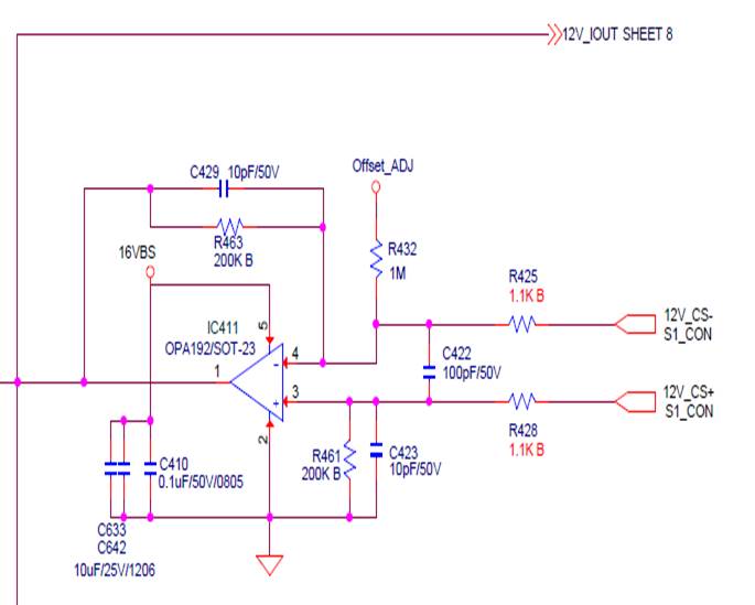
The test result is below:  CH4: Output current(3A-111A);  CH1: INA180A4 output  C422 = 100Pf, C423 = C421 = 1000pf

So here you can see the amplifier output will go to unstable oscillation. Do you have any suggestion about this unstable situation?

I also did some simulation about out part at this load transient condition: 3A-111A 10KHz:

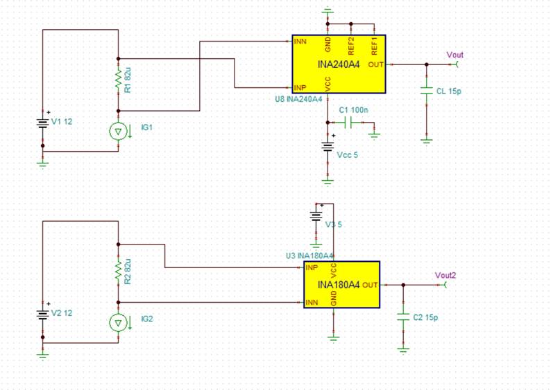
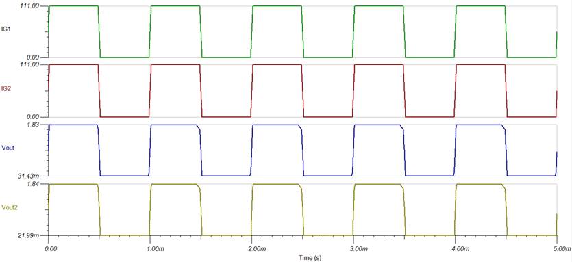
I didn't find any unstable issue here. So I can't understand what can lead our part to this issue. The input common mode cap and differential mode capacitor?

Any feedback are appreciated. Very urgent case.

Thanks

-Pengfei

  • Hi Pengfei,

    is the output of TPS70950 clean and free of oscillation?

    Or has it to do with this?

    e2e.ti.com/.../2547350

    See the note at the bottom of figure 45 of datasheet!

    Kai
  • I will check the RC circuit. How about the first static test issue?
    Thanks
    -Pengfei
  • Hi Pengfei,

    looks like a gain error due to a wrong shunt impedance. I guess it has to do with the unavoidable resistances of copper traces of printed circuit board running to the shunt. You could use 70µm FR4 or strenghten the copper traces by pieces of wire which you solder onto the copper traces running to the shunt. Keep in mind that also vias can have lots of resistance. They can be strenghtened by pieces of wire, too.

    Another method is, as you already suggested, to correct for the gain error in the software.

    Kai

  • Hey Pengfei,

    I am confused with the DC Error data plot. What is I_Share Spec? Is this supposed to be the VOUT for INA180? Should all the curves be the same? The output of the INA180 cannot exceed the supply voltage so I am confused when you show curves > 5V. To me the INA180A4 curve (blue line) actually seems to be close to what the ideal transfer curve should be. According to blue curve, the VOUT is ~2.4V at 135A load current. Ideally at 135A, VOUT = 135A*83.33µΩ*200 = 2.241V. Given the probable error due to your sense traces, I would say this is reasonable. Defintely probe the shunt resistors in different places as well as the sense resistance right at IN+, IN- pins and this should help debug your DC error. The customer does not seem to be using Kelvin sense connection that would remove any errors associated with solder resistance at pads of your shunts resistors. These connection require another pad that is not connected to the high-current bus line, but still makes contact with edge of the sense resistor.

    For the AC errors I would start debugging by removing all of the capacitors at the input of the INA180. I would also remove any capacitances from the output of INA180. Ensure the MCU ADC input is not causing any instability at INA180 output by disconnecting MCU and making measurement with oscilloscope probe.

    Best,

    Peter Iliya

    Current Sensing Applications

  • Hi Peter
    Thanks for your response.
    I_share Spec is their ideal value. Only the Blue line is INA180 Output. After the INA180, there is a amplifier circuit to amplify the INA180 output value.

    But you can just focus on the INA180 output(Blue line), the theoretical value is 3.0V, but now you can see the value has reached 3.2V. The customer requirement is that accuracy maximum is 2%(3V+/- 0.06V) at Full load (180A) and 10% error at 10% load(~20A). 3.2V is over their spec too much.
    You mentioned that customer did not use kelvin connection. Could you show what is the correct or better layout solution for our application to optimize their accuracy? Could you show some picture about what you said "These connection require another pad that is not connected to the high-current bus line, but still makes contact with edge of the sense resistor." I want to show our solution or suggestion to them. They put the DC issue at the first priority.
    They can calibrate by software. But when they make the full load accuracy better, the light load accuracy will be over their spec.So far we have no more idea to optimize the result.

    Could you comment the application circuit ? schematic or PCB layout suggestion.

    Wait for you about the AC test result.

    They have another one experience: they can use opa192(External Gain circuit) to fine tuning the gain resistor to reach their accuracy requirement.

    Any feedback are appreciated.
    Thanks
    -Pengfei
  • Hi Pengfei,

    Peter means that with such high currents you will need a shunt coming in a 4-terminal connection design.

    Such a shunt would work:

    Keep in mind that a typical solder joint alone can have a resistance of 100µ...1mOhm! Only be using such a 4-terminal connection shunt (Kelvin shunt) a precise measurement can be accomplished.

    Read very carefully section 11 of datasheet again and see how these 4-terminals are used.

    Kai

  • Pengfei,

    What are the tolerances of the shunt resistors?

    How are they using OPA192? Are they placing this at IC411 and creating a discrete differential amplifier? What resistor are the fine tuning?

    If each 0.5mΩ resistor is 1%, then putting 5 of these in parallel actually increases your total effective shunt resistor tolerance to SQRT(1^2+1+1+1+1) = 2.236% and this is assuming you have a perfect Kelvin sense connection, which customer has not implemented according to their layout. Customer must consider the total system error.

    In order to implement a Kelvin sense connection, you technically need 4 separate copper pads for each shunt resistor. Take for example the pad layout below for just one high power shunt resistor. In the layout below, one 0.5mΩ shunt resistor is soldered onto all four pads (1,2,3,4). Pads 2 and 3 are the sense pads while pads 1 and 4 the current-carrying pads. The high load current is to flow through pad 1+solder into resistor and then out of resistor and into solder+pad 4. Note that solder can contribute maybe 100µΩ of resistance to the shunt resistance. By sensing only off pads 2 and 3, the INA180 will only be sesning the voltage drop across the shunt resistor and not the extra soldering resistance at pads 1 and 4, which are carrying high-current and thus inducing an effectively larger shunt voltage drop.

    There are several ways/orientations you can position the sense pads, but the fundamentals are still the same. Customer needs to ensure they are achieving an actual 0.0833333mΩ sense resistance by applying a known current load and measuring the sense voltage directly with a multimeter.

    Hope this helps,

    Sincerely,

    Peter Iliya

  • Hi Peter,

    thanks for your support. About the opa192, they have two board. One is using opa192 which is an old design. the other one is using INA180 which is new design in. You can see the old schematic:

    They can tuning the R463, R425 or R461 , R428. For example,  If the accuracy can't meet their requirement, they can change R463 to 198k or lower. or change a little bit R425 to relize the proper accuracy.  I don't think it is correct way to optimize their system. I will promote our solution to them about what you mentioned. Have a look if we can solve their accuracy issue.

    One more point: the shunt resistor tolerance is one in a thousand。

    About the AC issue, hope you can still do some test to check the unstable cause.

    Thanks

    -Pengfei

  • Hi Pengfei,

    adjusting the resistor values in a dicrete design can work very well to enhance the common mode rejection. But this method costs time and efforts. It was the standard method when the INA weren't available and such amplifiers had to be build by the use of discretes.

    BUT: A careful analysis shows that even with a perfect trim the common mode rejection will drift with time and temperature. The best which can be achieved is about 50...60dB. No more. And only if the trimming is repeated in short intervals. A modern INA, on the other hand, provides a common mode rejection which is considerably higher. The INA180 offers a common mode rejection of more than 84dB, typically even 100dB! This is achieved by having all the components determining the common mode rejection fabricated on the same die. As they are fabricated in the same way by using the same materials they are nearly identical. And they are always having the same temperature. The use of an INA can mean a dramatical performance boost when it comes to common mode rejection!

    Kai
  • Hey Pengfei,

    Calibrating the OPA192 is one way to fix a shunt resistor layout sensing issue, but this cannot be done for INA180. The only way to ensure the sense connections to the shunt resistor are actually measuring a voltage drop across 0.0833mΩ is to use proper Kelvin sense pads as I described above. Or customer can just measure what the effective sense resistance is on there circuit (before populating INA180) and then use this to calibrate out DC errors.

    I cannot test for any possible AC errors because I do not know the layout, hardware, or full schematics. Is there anything else the INA180 is driving aside from MCU ADC port? Is there a charge-bucket RC filter at the ADC input? What is the sampling rate, conversion time, and acquisition time of the ADC, assuming it is a SAR ADC. These are the things that could be causing instability at INA180 output.

    Can customer probe with oscilloscope the VOUT of INA180 during DC testing to ensure there is no stability issue here?

    Has customer removed all capacitors at input of INA180 to see if this is not causing any AC issue?

    Sincerely,

    Peter Iliya

  • Hi Pengfei,

    It's been over two weeks since your last post, so it seems like your issue has been resolved. I will close the thread for now, but if you have any further questions you can reply to re-open it or start a new thread with a new question.

    Best regards,

    Ian Williams
    Applications Manager
    Current & Magnetic Sensing