This thread has been locked.

If you have a related question, please click the "Ask a related question" button in the top right corner. The newly created question will be automatically linked to this question.

LM358: Schematic review

Part Number: LM358


Hi
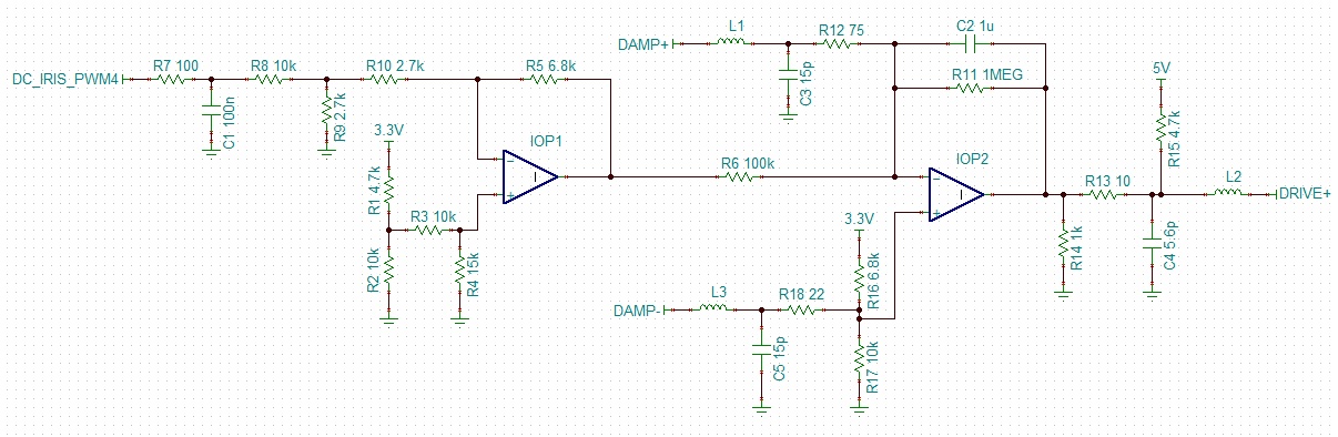
My client is developing a camera iris by completing the LM358.
The application part of the LM358PWR is the motor end of the iris.
Four defects occurred during the production of 200 units.
All the same symptoms that the waveform of OUT1 PIN is different from normal have occurred.
The faulty board is normally output when no load is applied, but the PWM signal is not output when a load (motor) is connected.
Could you give me advice on the Schematic?

DC_IRIS.pdf


please check.

  • Hi Kim,

    what a terrible schematic. No fun... :-(

    Without knowing what exactly is connected to the circuit at the left side and at the right side, it's nearly impossible to make a useful analysis!

    A bit strange is R181. It's only 75R and forms a huge gain in combination with R910=1M.

    And what is the purpose of R906=1k and R907=4k7?

    What is the supply voltage of LM358?

    Kai

  • Hi Andy,

    Like Kai said, can you detail the inputs and outputs? Any additional scope-shots or details that you can provide would be very useful. Please clarify what "the waveform of OUT1 PIN is different from normal have occurred" means. What is normal? What is different?

    I redrew the schematic in TINA - does this look correct?

    Here is the TINA file:

    LM358_Review.TSC

    Thank you,

    Paul

  • Kim,

    Are the DAMP+ DAMP- input sources AC coupled? If they are DC terminated then the op amp DC gain will be very high, 1Mohm/(75ohm + Rsource). Input offset voltage multiplied by the (gain +1) could put the first amplifier output beyond the linear range 0V to just over 3V. Please provide impedance of the DAMP signals, DC voltage on the op amps pins, and any relevant waveforms.

    There is also a new design app note for this op amp online.