This thread has been locked.

If you have a related question, please click the "Ask a related question" button in the top right corner. The newly created question will be automatically linked to this question.

TINA/Spice/THS4531A: Stability analysis with spice model

Part Number: THS4531A
Other Parts Discussed in Thread: TINA-TI, , THS4531

Tool/software: TINA-TI or Spice Models

Hello,

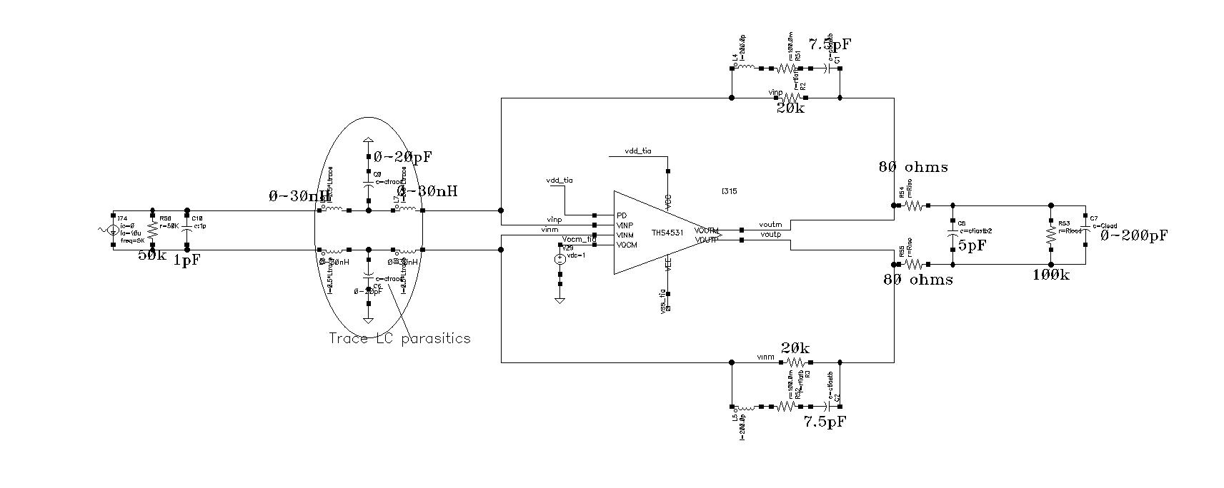
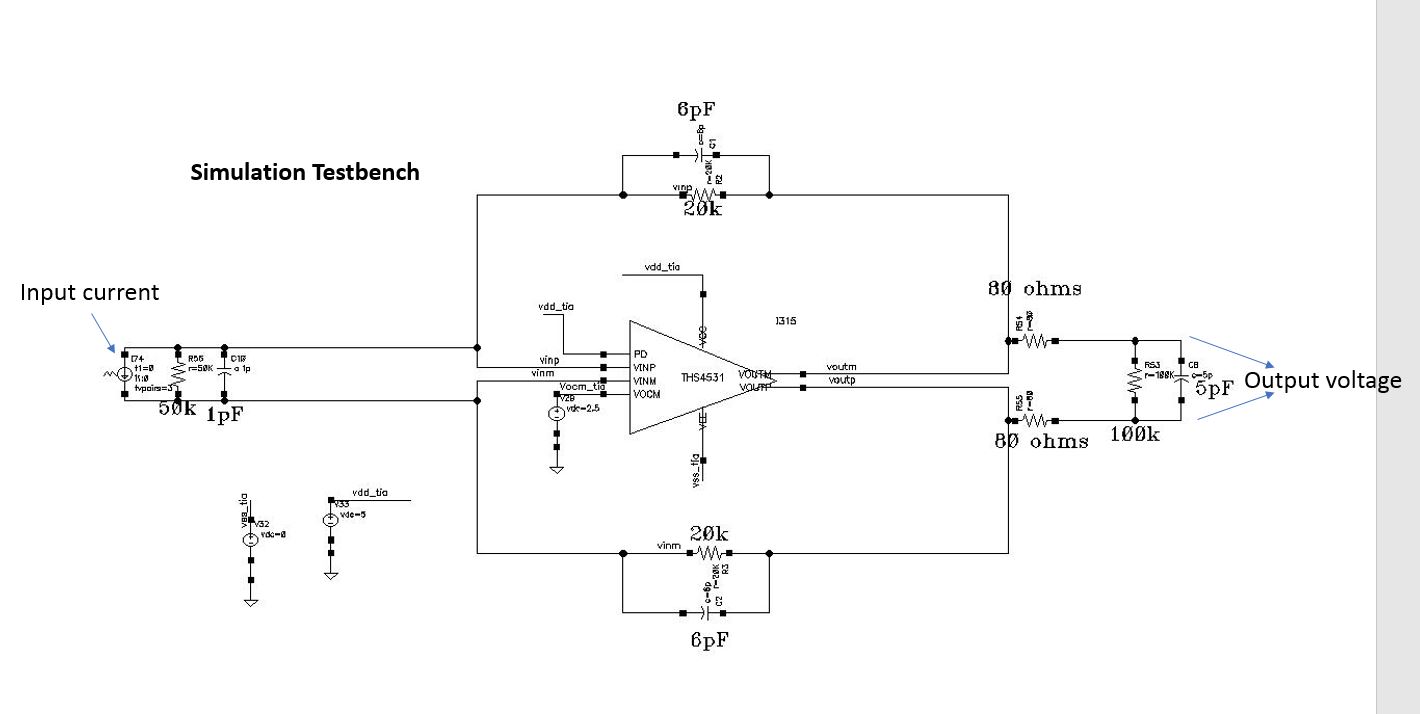
I am trying to  build a differential Transimpedence Amplifier with THS4531A.

I used a feedback resistor (which serves as Transimpedance) value of 20k in parallel with a compensation capacitor of 7.5pF

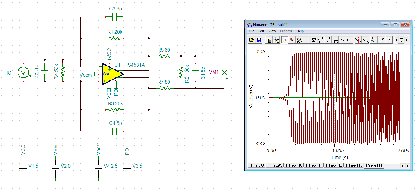
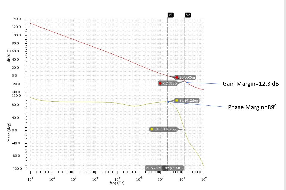
I used the pspice model for THS4531A in my Spectre simulations to check the stability. 

It gives me the phase margin ~ 72 degrees and Gain Margin ~ 16dB. which looks good enough to me.

My question is : Can I trust these spice models for the stability simulations I did in Spectre ?

regards,

Ashish

  • Hi Ashish,

    can you attach your TSC-file?

    Kai
  • Hello Kai,

    sorry for replying late as

    * THS4531
    *****************************************************************************
    * (C) Copyright 2011 Texas Instruments Incorporated. All rights reserved.������������������������������������������� 
    *****************************************************************************
    ** This model is designed as an aid for customers of Texas Instruments.
    ** TI and its licensors and suppliers make no warranties, either expressed
    ** or implied, with respect to this model, including the warranties of 
    ** merchantability or fitness for a particular purpose.� The model is
    ** provided solely on an "as is" basis.� The entire risk as to its quality
    ** and performance is with the customer.
    *****************************************************************************
    *]
    ** Released by: Analog eLab Design Center, Texas Instruments Inc.
    * Part: THS4531
    * Date: 04NOV2011
    * Model Type: ALL-IN-ONE
    * Simulator: PSPICE
    * Simulator Version: 16.0.0.p001
    * EVM Order Number: N/A
    * EVM Users Guide: N/A
    * Datasheet: SLOS358 - SEPTEMBER 2011
    *
    * Model Version: 1.0
    *
    *****************************************************************************
    *
    * Updates:
    *
    * Version 1.0 : 
    * Release to Web
    *
    *****************************************************************************
    *
    
    * BEGIN FEATURES
    * 5V Supply only
    * OPEN LOOP GAIN AND PHASE
    * INPUT VOLTAGE NOISE
    * UGBW
    * INPUT COMMON MODE VOLTAGE RANGE
    * SLEW RATE
    * tr and tf
    * QUIESCENT CURRENT ON mode
    * QUIESCENT CURRENT OFF mode
    * OUTPUT CLAMPS TO RAILS
    * PWD Mode
    * END FEATURES
    
    * source THS4531
    *$
    .SUBCKT THS4531 VIN+ VIN- VOCM VCC VEE VOUT+ VOUT- PD
    V_V17         N3337259 VZNEG DC 0 AC 0 0
    Q_Q2         N3339183 VIN- N3338287 TI_PNP 
    R_R29         VMID VZPOS  330k  
    R_R6         N3338225 VCCX  2.5k  
    C_C11         0 N3336111  400f  
    X_F9    N3339183 VEEX N3337259 VEEX THS4531_F9 
    E_E1         N3340803 0 VMID VZNEG 1
    Q_Q14         VEEX VOCM N3336085 TI_PNP 
    R_R17         VEEX N3339341  3k  
    R_R27         N3336827 N3338503  200  
    V_V4         N3336157 VEE 0.95Vdc
    R_R20         VEE VOCM  10G  
    V_V3         N3339361 VEE 0.95Vdc
    E_E4         N3336659 0 VMID VZPOS 1
    D_U3         VCCX N3339177 TI_D 
    X_F1    N3336787 VEEX IQBN VEEX THS4531_F1 
    V_V6         VVG N3338333 100mVdc
    X_F4    VCCX N3338993 VZPOS VEEX THS4531_F4 
    Q_Q25         IBMAIN N3336839 VEEX TI_NPN 
    V_V11         VIN+ N3373550 0.1m
    R_R24         0 N3336827  570k  
    C_C6         N3336827 VZNEG  5.0p  
    Q_Q24         N3336839 N3336839 N3337249 TI_NPN 
    R_R15         N3338215 VCCX  3k  
    X_F10    IBMAIN IQB1 VCCX N3337259 THS4531_F10 
    X_S1    PD 0 S1_2_DRAIN N3340899 THS4531_S1 
    X_S6    N3338119 0 N3338119 N3338383 THS4531_S6 
    D_D14         N3336827 N3338483 TI_D 
    Q_Q26         PDZ PD VEEX TI_NPN 
    Q_Q15         VCCX VOCM N3338961 TI_NPN 
    C_C9         N3336111 VZPOS  5.0p  
    Q_Q17         VEEX N3338961 N3337145 TI_PNP 
    Q_Q23         N3336085 N3337083 N3338215 TI_PNP 
    V_V14         N3340585 VEE 0Vdc
    X_F7    IQBE IQBF N3337083 N3338645 THS4531_F7 
    D_D17         N3336111 N3341133 TI_D 
    C_C2         0 N3336827  400f  
    R_R23         0 N3339173  400k  
    R_R36         PD VCC  10G  
    G_G5         N3338993 N3338999 N3337145 N3336983 2e-3
    E_E11         VEEX 0 VEE 0 1
    Q_Q5         VVG IBMAIN N3338639 TI_PNP 
    E_E7         N3338119 0 VIN+ VIN- -1
    Q_Q16         VCCX N3336085 N3337145 TI_NPN 
    D_D15         N3339361 N3336827 TI_D 
    X_F8    N3339467 VEEX N3339459 VEEX THS4531_F8 
    Q_Q10         PDZ PD VCCX TI_PNP 
    C_C7         0 N3336145  100f  
    R_R37         VCC S1_2_DRAIN  20k  
    X_F13    IQB1 IQB7 VCCX N3339459 THS4531_F13 
    X_S9    PD 0 N3336111 VOUT- THS4531_S9 
    V_V5         VCC N3341133 0.95Vdc
    D_U2         VCCX N3338639 TI_D 
    X_S4    PDZ 0 S3_4_DRAIN N3340585 THS4531_S4 
    G_G2         N3336827 0 N3339173 0 4e-3
    X_U6         N3338639 VCCX RNL PARAMS:  R=2.5k
    C_C8         N3336111 N3336145  250f  
    X_F2    IQBL IQBN VCCX IBMAIN THS4531_F2 
    C_C17         N3336983 VCCX  20f  
    X_U4         N3373550 N3338527 vnse PARAMS:
    R_R33         N3339187 VCCX  10Meg  
    X_S11    PDZ 0 VOUT- VOCM THS4531_S11 
    C_C4         VMID VZNEG  50f  
    C_C3         N3336827 N3339173  250f  
    E_E5         VREF 0 N3339187 0 1
    X_U7         N3339177 VCCX RNL PARAMS:  R=2.5k
    X_S12    PDZ 0 VOCM VOUT+ THS4531_S12 
    C_C1         0 N3339173  100f  
    Q_Q9         VVG IBMAIN N3339177 TI_PNP 
    G_G1         N3339173 0 N3340803 0 0.85e-3
    E_E6         N3337827 0 VIN+ VIN- 1
    R_R14         N3337087 VCCX  3k  
    R_R35         VABS N3338383  1000  
    V_V7         VVG N3338287 100mVdc
    E_E10         VCCX 0 VCC 0 1
    C_C16         VEEX N3336983  20f  
    R_R25         VMID VZNEG  330k  
    I_I2         VCC S3_4_DRAIN DC 20nAdc  
    R_R34         VEEX N3339187  10Meg  
    R_R28         0 N3336145  400k  
    R_R30         N3336111 N3338323  200  
    C_C18         0 VABS  1p  
    E_E14         VMID VEE VCC VEE 0.5
    X_S10    PD 0 N3336827 VOUT+ THS4531_S10 
    Q_Q22         N3337083 N3337083 N3337087 TI_PNP 
    D_U1         VCCX N3338225 TI_D 
    V_V2         VCC N3338483 0.95Vdc
    X_F5    N3338999 VEEX VZNEG VEEX THS4531_F5 
    X_F3    IQB7 IQBE VCCX VEEX THS4531_F3 
    V_V12         N3340899 VEE 0Vdc
    E_E15         N3337249 VEEX VABS 0 0.102
    I_I1         VCCX N3336787 DC 30uAdc  
    X_F6    IQBF IQBL VCCX N3336839 THS4531_F6 
    Q_Q19         N3338961 N3338645 N3339341 TI_NPN 
    D_D16         N3336157 N3336111 TI_D 
    R_R21         N3336983 VOUT+  100K  
    G_G3         N3336111 0 N3336145 0 4e-3
    R_R16         VEEX N3336629  3k  
    R_R31         0 N3336111  570k  
    V_V18         N3339459 VZPOS DC 0 AC 0 0
    Q_Q1         N3339467 N3338527 N3338333 TI_PNP 
    Q_Q8         IBMAIN IBMAIN N3338225 TI_PNP 
    X_S5    N3337827 0 N3337827 N3338383 THS4531_S5 
    C_C10         VMID VZPOS  50f  
    Q_Q18         N3338645 N3338645 N3336629 TI_NPN 
    R_R19         VOCM VCC  10G  
    R_R22         VOUT- N3336983  100K  
    C_C13         N3338323 N3338503  40p  
    G_G4         N3336145 0 N3336659 0 0.85e-3
    .ENDS
    *$
    * END MODEL THS4531
    .subckt THS4531_F9 1 2 3 4  
    F_F9         3 4 VF_F9 1
    VF_F9         1 2 0V
    .ends THS4531_F9
    *$
    .subckt THS4531_F1 1 2 3 4  
    F_F1         3 4 VF_F1 1
    VF_F1         1 2 0V
    .ends THS4531_F1
    *$
    .subckt THS4531_F4 1 2 3 4  
    F_F4         3 4 VF_F4 1
    VF_F4         1 2 0V
    .ends THS4531_F4
    *$
    .subckt THS4531_F10 1 2 3 4  
    F_F10         3 4 VF_F10 1
    VF_F10         1 2 0V
    .ends THS4531_F10
    *$
    .subckt THS4531_S1 1 2 3 4  
    S_S1         3 4 1 2 _S1
    RS_S1         1 2 1G
    .MODEL         _S1 VSWITCH Roff=10e9 Ron=1.0m VH=0.3V VT=1.0V TD=0
    .ends THS4531_S1
    *$
    .subckt THS4531_S6 1 2 3 4  
    S_S6         3 4 1 2 _S6
    RS_S6         1 2 1G
    .MODEL         _S6 VSWITCH Roff=1e6 Ron=1.0 Voff=0.0V Von=1e-1
    .ends THS4531_S6
    *$
    .subckt THS4531_F7 1 2 3 4  
    F_F7         3 4 VF_F7 1.2
    VF_F7         1 2 0V
    .ends THS4531_F7
    *$
    .subckt THS4531_F8 1 2 3 4  
    F_F8         3 4 VF_F8 1
    VF_F8         1 2 0V
    .ends THS4531_F8
    *$
    .subckt THS4531_F13 1 2 3 4  
    F_F13         3 4 VF_F13 1
    VF_F13         1 2 0V
    .ends THS4531_F13
    *$
    .subckt THS4531_S9 1 2 3 4  
    S_S9         3 4 1 2 _S9
    RS_S9         1 2 1G
    .MODEL         _S9 VSWITCH Roff=10e6 Ron=1.0e-3 VH=0.3V VT=1.0V TD=0
    .ends THS4531_S9
    *$
    .subckt THS4531_S4 1 2 3 4  
    S_S4         3 4 1 2 _S4
    RS_S4         1 2 1G
    .MODEL         _S4 VSWITCH Roff=10e6 Ron=1.0e-3 VH=0.3V VT=1.0V TD=0
    .ends THS4531_S4
    *$
    .subckt THS4531_F2 1 2 3 4  
    F_F2         3 4 VF_F2 1
    VF_F2         1 2 0V
    .ends THS4531_F2
    *$
    .subckt THS4531_S11 1 2 3 4  
    S_S11         3 4 1 2 _S11
    RS_S11         1 2 1G
    .MODEL         _S11 VSWITCH Roff=10e6 Ron=1.0e-3 VH=0.3V VT=1.0V TD=0
    .ends THS4531_S11
    *$
    .subckt THS4531_S12 1 2 3 4  
    S_S12         3 4 1 2 _S12
    RS_S12         1 2 1G
    .MODEL         _S12 VSWITCH Roff=10e6 Ron=1.0e-3 VH=0.3V VT=1.0V TD=0
    .ends THS4531_S12
    *$
    .subckt THS4531_S10 1 2 3 4  
    S_S10         3 4 1 2 _S10
    RS_S10         1 2 1G
    .MODEL         _S10 VSWITCH Roff=10e6 Ron=1.0e-3 VH=0.3V VT=1.0V TD=0
    .ends THS4531_S10
    *$
    .subckt THS4531_F5 1 2 3 4  
    F_F5         3 4 VF_F5 1
    VF_F5         1 2 0V
    .ends THS4531_F5
    *$
    .subckt THS4531_F3 1 2 3 4  
    F_F3         3 4 VF_F3 2
    VF_F3         1 2 0V
    .ends THS4531_F3
    *$
    .subckt THS4531_F6 1 2 3 4  
    F_F6         3 4 VF_F6 1
    VF_F6         1 2 0V
    .ends THS4531_F6
    *$
    .subckt THS4531_S5 1 2 3 4  
    S_S5         3 4 1 2 _S5
    RS_S5         1 2 1G
    .MODEL         _S5 VSWITCH Roff=1e6 Ron=1.0 Voff=0.0V Von=1e-1
    .ends THS4531_S5
    *$
    ** Wrapper definitions for AA legacy support **
    .model TI_PNP pnp
    + bf=150
    + va=120
    + rb=440
    + re=20
    + tf=2e-013
    + cjc=1e-013
    + cje=1e-013
    + kf=8.8e-015
    *$
    .model TI_D d
    + is=1e-013
    + vj=0.4
    + cjo=6e-013
    *$
    .model TI_NPN npn
    + bf=150
    + va=120
    + rb=190
    + re=20
    + tf=2e-013
    + cjc=1e-013
    + cje=1e-013
    + kf=5.3e-015
    *$
    *******************************************************
    *******************************************************
    
    .subckt RNL a b PARAMS: R=1k
    *H_H1 c b VH_H1 {R}
    *VH_H1 a c 0
    ERES a 3 VALUE = { I(VSENSE) * R }
    Rdummy 30 3 1
    VSENSE 30 b DC 0V
    .ends
    
    *******************************************************
    
    
    .SUBCKT VNSE 1 2 
    **************************
    * BEGIN SETUP OF NOISE GEN - NANOVOLT/RT-HZ
    * INPUT THREE VARIABLES
    * NLF - NV/RHZ AT (1/F) FREQ
    * FLW - FREQ FOR (1/F) VAL
    * NVR - NV/RHZ FLATBAND
    **************************
    * START CALC VALS
    .PARAM NLF=5
    .PARAM FLW=1
    .PARAM NVR=7.0
    .PARAM GLF={PWR(FLW,0.25)*NLF/1164}
    .PARAM RNV={1.184*PWR(NVR,2)}
    .MODEL DVN D KF={PWR(FLW,0.5)/1E11} IS=1.0E-16
    * END CALC VALS
    I1 0 7 10E-3
    I2 0 8 10E-3
    D1 7 0 DVN
    D2 8 0 DVN
    E1 3 6 7 8 {GLF}
    R1 3 0 1E9
    R2 3 0 1E9
    R3 3 6 1E9
    E2 6 4 5 0 10
    R4 5 0 {RNV}
    R5 5 0 {RNV}
    R6 3 4 1E9
    R7 4 0 1E9
    E3 1 2 3 4 1
    C1 1 0 1E-15
    C2 2 0 1E-15
    C3 1 2 1E-15
    .ENDS VNSE
    *******************************************************
    *$
    
     ran into more stability issues with the transimpedance amplifier I so designed.

    I am running Spectre simulation with the pspice model of THS4531A. Hence I don't have the TSC file. I am attaching the spectre simulation file (input_scs.txt), the p-spice model for THS4531A (ths4531_lib.txt) and the snapshot of the Transimpedence amplifier schematic I am using for my stability simualtions (TIA.jpg).

    Please let me know if this helps.

    regards,

    Ashish

  • // Generated for: spectre
    // Generated on: Mar  1 09:51:37 2019
    // Design library name: amos_abcd9_cur_sense_lib_tb_ap
    // Design cell name: tb_idealinput_tia
    // Design view name: schematic
    simulator lang=spectre
    global 0
    parameters ctiastb3=2e-15 ctiastb2=4p ctrace=1e-15 Ltrace=60e-9 \
        Cload=5e-15 ctiastb=9p Riso=80 Rload=100000 rtiafb=20000 rcsbout=4000
    
    pspice_include "./ths4531_lib.txt"
    
    // Library name: analogLib
    // Cell name: ideal_balun
    // View name: schematic
    subckt ideal_balun d c p n
        K0 (d 0 p c) transformer n1=2
        K1 (d 0 c n) transformer n1=2
    ends ideal_balun
    // End of subcircuit definition.
    
    // Library name: amos_abcd9_cur_sense_lib_tb_ap
    // Cell name: tb_idealinput_tia
    // View name: schematic
    I65 (voutm voutp net064 net063) diffstbprobe
    V32 (vss_tia 0) vsource dc=0 type=dc
    V33 (vdd_tia 0) vsource dc=2.5 type=dc
    V29 (Vocm_tia 0) vsource dc=1 type=dc
    I315 (vinp vinm Vocm_tia vdd_tia vss_tia voutp voutm vdd_tia) THS4531
    R53 (net023 net022) resistor r=Rload isnoisy=no
    R56 (net011 net010) resistor r=50K
    R46 (voutm modoutn) resistor r=1
    R51 (net091 net092) resistor r=100.0m
    R52 (net070 net093) resistor r=100.0m
    R54 (net064 net023) resistor r=Riso isnoisy=no
    R55 (net063 net022) resistor r=Riso isnoisy=no
    R3 (net063 vinm) resistor r=rtiafb isnoisy=no
    R2 (net064 vinp) resistor r=rtiafb isnoisy=no
    R44 (csoutn vinm) resistor r=1
    R43 (csoutp vinp) resistor r=1
    R45 (voutp modoutp) resistor r=1
    I74 (net011 net010) isource dc=0 type=sine sinedc=0 ampl=10u freq=5K
    E27 (net090 0 csoutn 0) vcvs gain=1
    E28 (net089 0 csoutp 0) vcvs gain=1
    E29 (modoutdiff 0 modoutp modoutn) vcvs gain=1
    L8 (net010 net01) inductor l=0.5*Ltrace
    L6 (net011 net02) inductor l=0.5*Ltrace
    L9 (net01 csoutn) inductor l=0.5*Ltrace
    L7 (net02 csoutp) inductor l=0.5*Ltrace
    L4 (vinp net092) inductor l=200.0p
    L5 (vinm net093) inductor l=200.0p
    C7 (net023 net022) capacitor c=Cload
    C6 (0 net01) capacitor c=ctrace
    C0 (0 net02) capacitor c=ctrace
    C1 (net064 net091) capacitor c=ctiastb
    C2 (net063 net070) capacitor c=ctiastb
    C8 (net023 net022) capacitor c=ctiastb2
    C10 (net011 net010) capacitor c=1p
    E9 (modoutdiff_A_weight 0 modoutdiff 0) svcvs gain=7.39705e9 poles=[ \
            -129.4 0 -129.4 0 -676.7 0 -4636 0 -76655 0 -76655 0 ] zeros=[ 0 0 \
            0 0 0 0 0 0 ]
    I32 (csoutdiff csoutcm net089 net090) ideal_balun
    simulatorOptions options reltol=1e-3 vabstol=1e-6 iabstol=1e-12 temp=27 \
        tnom=27 scalem=1.0 scale=1.0 gmin=1e-12 rforce=1 maxnotes=5 maxwarns=5 \
        digits=5 cols=80 pivrel=1e-3 sensfile="../psf/sens.output" \
        checklimitdest=psf 
    stb stb start=1 stop=1e9 probe=I65.IPRB_DM annotate=status 
    saveOptions options save=lvlpub nestlvl=1
    include \
            "/sysmnt/cadappl_sde/ictools/cadence_ic/6.1.7.500.14/tools/dfII/etc/cdslib/artist/analogLib/diffstbprobe/diffstbprobe.scs"
    

  • * THS4531
    *****************************************************************************
    * (C) Copyright 2011 Texas Instruments Incorporated. All rights reserved.������������������������������������������� 
    *****************************************************************************
    ** This model is designed as an aid for customers of Texas Instruments.
    ** TI and its licensors and suppliers make no warranties, either expressed
    ** or implied, with respect to this model, including the warranties of 
    ** merchantability or fitness for a particular purpose.� The model is
    ** provided solely on an "as is" basis.� The entire risk as to its quality
    ** and performance is with the customer.
    *****************************************************************************
    *]
    ** Released by: Analog eLab Design Center, Texas Instruments Inc.
    * Part: THS4531
    * Date: 04NOV2011
    * Model Type: ALL-IN-ONE
    * Simulator: PSPICE
    * Simulator Version: 16.0.0.p001
    * EVM Order Number: N/A
    * EVM Users Guide: N/A
    * Datasheet: SLOS358 - SEPTEMBER 2011
    *
    * Model Version: 1.0
    *
    *****************************************************************************
    *
    * Updates:
    *
    * Version 1.0 : 
    * Release to Web
    *
    *****************************************************************************
    *
    
    * BEGIN FEATURES
    * 5V Supply only
    * OPEN LOOP GAIN AND PHASE
    * INPUT VOLTAGE NOISE
    * UGBW
    * INPUT COMMON MODE VOLTAGE RANGE
    * SLEW RATE
    * tr and tf
    * QUIESCENT CURRENT ON mode
    * QUIESCENT CURRENT OFF mode
    * OUTPUT CLAMPS TO RAILS
    * PWD Mode
    * END FEATURES
    
    * source THS4531
    *$
    .SUBCKT THS4531 VIN+ VIN- VOCM VCC VEE VOUT+ VOUT- PD
    V_V17         N3337259 VZNEG DC 0 AC 0 0
    Q_Q2         N3339183 VIN- N3338287 TI_PNP 
    R_R29         VMID VZPOS  330k  
    R_R6         N3338225 VCCX  2.5k  
    C_C11         0 N3336111  400f  
    X_F9    N3339183 VEEX N3337259 VEEX THS4531_F9 
    E_E1         N3340803 0 VMID VZNEG 1
    Q_Q14         VEEX VOCM N3336085 TI_PNP 
    R_R17         VEEX N3339341  3k  
    R_R27         N3336827 N3338503  200  
    V_V4         N3336157 VEE 0.95Vdc
    R_R20         VEE VOCM  10G  
    V_V3         N3339361 VEE 0.95Vdc
    E_E4         N3336659 0 VMID VZPOS 1
    D_U3         VCCX N3339177 TI_D 
    X_F1    N3336787 VEEX IQBN VEEX THS4531_F1 
    V_V6         VVG N3338333 100mVdc
    X_F4    VCCX N3338993 VZPOS VEEX THS4531_F4 
    Q_Q25         IBMAIN N3336839 VEEX TI_NPN 
    V_V11         VIN+ N3373550 0.1m
    R_R24         0 N3336827  570k  
    C_C6         N3336827 VZNEG  5.0p  
    Q_Q24         N3336839 N3336839 N3337249 TI_NPN 
    R_R15         N3338215 VCCX  3k  
    X_F10    IBMAIN IQB1 VCCX N3337259 THS4531_F10 
    X_S1    PD 0 S1_2_DRAIN N3340899 THS4531_S1 
    X_S6    N3338119 0 N3338119 N3338383 THS4531_S6 
    D_D14         N3336827 N3338483 TI_D 
    Q_Q26         PDZ PD VEEX TI_NPN 
    Q_Q15         VCCX VOCM N3338961 TI_NPN 
    C_C9         N3336111 VZPOS  5.0p  
    Q_Q17         VEEX N3338961 N3337145 TI_PNP 
    Q_Q23         N3336085 N3337083 N3338215 TI_PNP 
    V_V14         N3340585 VEE 0Vdc
    X_F7    IQBE IQBF N3337083 N3338645 THS4531_F7 
    D_D17         N3336111 N3341133 TI_D 
    C_C2         0 N3336827  400f  
    R_R23         0 N3339173  400k  
    R_R36         PD VCC  10G  
    G_G5         N3338993 N3338999 N3337145 N3336983 2e-3
    E_E11         VEEX 0 VEE 0 1
    Q_Q5         VVG IBMAIN N3338639 TI_PNP 
    E_E7         N3338119 0 VIN+ VIN- -1
    Q_Q16         VCCX N3336085 N3337145 TI_NPN 
    D_D15         N3339361 N3336827 TI_D 
    X_F8    N3339467 VEEX N3339459 VEEX THS4531_F8 
    Q_Q10         PDZ PD VCCX TI_PNP 
    C_C7         0 N3336145  100f  
    R_R37         VCC S1_2_DRAIN  20k  
    X_F13    IQB1 IQB7 VCCX N3339459 THS4531_F13 
    X_S9    PD 0 N3336111 VOUT- THS4531_S9 
    V_V5         VCC N3341133 0.95Vdc
    D_U2         VCCX N3338639 TI_D 
    X_S4    PDZ 0 S3_4_DRAIN N3340585 THS4531_S4 
    G_G2         N3336827 0 N3339173 0 4e-3
    X_U6         N3338639 VCCX RNL PARAMS:  R=2.5k
    C_C8         N3336111 N3336145  250f  
    X_F2    IQBL IQBN VCCX IBMAIN THS4531_F2 
    C_C17         N3336983 VCCX  20f  
    X_U4         N3373550 N3338527 vnse PARAMS:
    R_R33         N3339187 VCCX  10Meg  
    X_S11    PDZ 0 VOUT- VOCM THS4531_S11 
    C_C4         VMID VZNEG  50f  
    C_C3         N3336827 N3339173  250f  
    E_E5         VREF 0 N3339187 0 1
    X_U7         N3339177 VCCX RNL PARAMS:  R=2.5k
    X_S12    PDZ 0 VOCM VOUT+ THS4531_S12 
    C_C1         0 N3339173  100f  
    Q_Q9         VVG IBMAIN N3339177 TI_PNP 
    G_G1         N3339173 0 N3340803 0 0.85e-3
    E_E6         N3337827 0 VIN+ VIN- 1
    R_R14         N3337087 VCCX  3k  
    R_R35         VABS N3338383  1000  
    V_V7         VVG N3338287 100mVdc
    E_E10         VCCX 0 VCC 0 1
    C_C16         VEEX N3336983  20f  
    R_R25         VMID VZNEG  330k  
    I_I2         VCC S3_4_DRAIN DC 20nAdc  
    R_R34         VEEX N3339187  10Meg  
    R_R28         0 N3336145  400k  
    R_R30         N3336111 N3338323  200  
    C_C18         0 VABS  1p  
    E_E14         VMID VEE VCC VEE 0.5
    X_S10    PD 0 N3336827 VOUT+ THS4531_S10 
    Q_Q22         N3337083 N3337083 N3337087 TI_PNP 
    D_U1         VCCX N3338225 TI_D 
    V_V2         VCC N3338483 0.95Vdc
    X_F5    N3338999 VEEX VZNEG VEEX THS4531_F5 
    X_F3    IQB7 IQBE VCCX VEEX THS4531_F3 
    V_V12         N3340899 VEE 0Vdc
    E_E15         N3337249 VEEX VABS 0 0.102
    I_I1         VCCX N3336787 DC 30uAdc  
    X_F6    IQBF IQBL VCCX N3336839 THS4531_F6 
    Q_Q19         N3338961 N3338645 N3339341 TI_NPN 
    D_D16         N3336157 N3336111 TI_D 
    R_R21         N3336983 VOUT+  100K  
    G_G3         N3336111 0 N3336145 0 4e-3
    R_R16         VEEX N3336629  3k  
    R_R31         0 N3336111  570k  
    V_V18         N3339459 VZPOS DC 0 AC 0 0
    Q_Q1         N3339467 N3338527 N3338333 TI_PNP 
    Q_Q8         IBMAIN IBMAIN N3338225 TI_PNP 
    X_S5    N3337827 0 N3337827 N3338383 THS4531_S5 
    C_C10         VMID VZPOS  50f  
    Q_Q18         N3338645 N3338645 N3336629 TI_NPN 
    R_R19         VOCM VCC  10G  
    R_R22         VOUT- N3336983  100K  
    C_C13         N3338323 N3338503  40p  
    G_G4         N3336145 0 N3336659 0 0.85e-3
    .ENDS
    *$
    * END MODEL THS4531
    .subckt THS4531_F9 1 2 3 4  
    F_F9         3 4 VF_F9 1
    VF_F9         1 2 0V
    .ends THS4531_F9
    *$
    .subckt THS4531_F1 1 2 3 4  
    F_F1         3 4 VF_F1 1
    VF_F1         1 2 0V
    .ends THS4531_F1
    *$
    .subckt THS4531_F4 1 2 3 4  
    F_F4         3 4 VF_F4 1
    VF_F4         1 2 0V
    .ends THS4531_F4
    *$
    .subckt THS4531_F10 1 2 3 4  
    F_F10         3 4 VF_F10 1
    VF_F10         1 2 0V
    .ends THS4531_F10
    *$
    .subckt THS4531_S1 1 2 3 4  
    S_S1         3 4 1 2 _S1
    RS_S1         1 2 1G
    .MODEL         _S1 VSWITCH Roff=10e9 Ron=1.0m VH=0.3V VT=1.0V TD=0
    .ends THS4531_S1
    *$
    .subckt THS4531_S6 1 2 3 4  
    S_S6         3 4 1 2 _S6
    RS_S6         1 2 1G
    .MODEL         _S6 VSWITCH Roff=1e6 Ron=1.0 Voff=0.0V Von=1e-1
    .ends THS4531_S6
    *$
    .subckt THS4531_F7 1 2 3 4  
    F_F7         3 4 VF_F7 1.2
    VF_F7         1 2 0V
    .ends THS4531_F7
    *$
    .subckt THS4531_F8 1 2 3 4  
    F_F8         3 4 VF_F8 1
    VF_F8         1 2 0V
    .ends THS4531_F8
    *$
    .subckt THS4531_F13 1 2 3 4  
    F_F13         3 4 VF_F13 1
    VF_F13         1 2 0V
    .ends THS4531_F13
    *$
    .subckt THS4531_S9 1 2 3 4  
    S_S9         3 4 1 2 _S9
    RS_S9         1 2 1G
    .MODEL         _S9 VSWITCH Roff=10e6 Ron=1.0e-3 VH=0.3V VT=1.0V TD=0
    .ends THS4531_S9
    *$
    .subckt THS4531_S4 1 2 3 4  
    S_S4         3 4 1 2 _S4
    RS_S4         1 2 1G
    .MODEL         _S4 VSWITCH Roff=10e6 Ron=1.0e-3 VH=0.3V VT=1.0V TD=0
    .ends THS4531_S4
    *$
    .subckt THS4531_F2 1 2 3 4  
    F_F2         3 4 VF_F2 1
    VF_F2         1 2 0V
    .ends THS4531_F2
    *$
    .subckt THS4531_S11 1 2 3 4  
    S_S11         3 4 1 2 _S11
    RS_S11         1 2 1G
    .MODEL         _S11 VSWITCH Roff=10e6 Ron=1.0e-3 VH=0.3V VT=1.0V TD=0
    .ends THS4531_S11
    *$
    .subckt THS4531_S12 1 2 3 4  
    S_S12         3 4 1 2 _S12
    RS_S12         1 2 1G
    .MODEL         _S12 VSWITCH Roff=10e6 Ron=1.0e-3 VH=0.3V VT=1.0V TD=0
    .ends THS4531_S12
    *$
    .subckt THS4531_S10 1 2 3 4  
    S_S10         3 4 1 2 _S10
    RS_S10         1 2 1G
    .MODEL         _S10 VSWITCH Roff=10e6 Ron=1.0e-3 VH=0.3V VT=1.0V TD=0
    .ends THS4531_S10
    *$
    .subckt THS4531_F5 1 2 3 4  
    F_F5         3 4 VF_F5 1
    VF_F5         1 2 0V
    .ends THS4531_F5
    *$
    .subckt THS4531_F3 1 2 3 4  
    F_F3         3 4 VF_F3 2
    VF_F3         1 2 0V
    .ends THS4531_F3
    *$
    .subckt THS4531_F6 1 2 3 4  
    F_F6         3 4 VF_F6 1
    VF_F6         1 2 0V
    .ends THS4531_F6
    *$
    .subckt THS4531_S5 1 2 3 4  
    S_S5         3 4 1 2 _S5
    RS_S5         1 2 1G
    .MODEL         _S5 VSWITCH Roff=1e6 Ron=1.0 Voff=0.0V Von=1e-1
    .ends THS4531_S5
    *$
    ** Wrapper definitions for AA legacy support **
    .model TI_PNP pnp
    + bf=150
    + va=120
    + rb=440
    + re=20
    + tf=2e-013
    + cjc=1e-013
    + cje=1e-013
    + kf=8.8e-015
    *$
    .model TI_D d
    + is=1e-013
    + vj=0.4
    + cjo=6e-013
    *$
    .model TI_NPN npn
    + bf=150
    + va=120
    + rb=190
    + re=20
    + tf=2e-013
    + cjc=1e-013
    + cje=1e-013
    + kf=5.3e-015
    *$
    *******************************************************
    *******************************************************
    
    .subckt RNL a b PARAMS: R=1k
    *H_H1 c b VH_H1 {R}
    *VH_H1 a c 0
    ERES a 3 VALUE = { I(VSENSE) * R }
    Rdummy 30 3 1
    VSENSE 30 b DC 0V
    .ends
    
    *******************************************************
    
    
    .SUBCKT VNSE 1 2 
    **************************
    * BEGIN SETUP OF NOISE GEN - NANOVOLT/RT-HZ
    * INPUT THREE VARIABLES
    * NLF - NV/RHZ AT (1/F) FREQ
    * FLW - FREQ FOR (1/F) VAL
    * NVR - NV/RHZ FLATBAND
    **************************
    * START CALC VALS
    .PARAM NLF=5
    .PARAM FLW=1
    .PARAM NVR=7.0
    .PARAM GLF={PWR(FLW,0.25)*NLF/1164}
    .PARAM RNV={1.184*PWR(NVR,2)}
    .MODEL DVN D KF={PWR(FLW,0.5)/1E11} IS=1.0E-16
    * END CALC VALS
    I1 0 7 10E-3
    I2 0 8 10E-3
    D1 7 0 DVN
    D2 8 0 DVN
    E1 3 6 7 8 {GLF}
    R1 3 0 1E9
    R2 3 0 1E9
    R3 3 6 1E9
    E2 6 4 5 0 10
    R4 5 0 {RNV}
    R5 5 0 {RNV}
    R6 3 4 1E9
    R7 4 0 1E9
    E3 1 2 3 4 1
    C1 1 0 1E-15
    C2 2 0 1E-15
    C3 1 2 1E-15
    .ENDS VNSE
    *******************************************************
    *$
    

  • Hello Kai,
    Reframing my earlier reply which was distorted after I tried to attach the files.:

    Sorry for replying late as I ran into more stability issues with the transimpedance amplifier I so designed.

    I am running Spectre simulation with the pspice model of THS4531A. Hence I don't have the TSC file. I am attaching the spectre simulation file (input_scs.txt), the p-spice model for THS4531A (ths4531_lib.txt) and the snapshot of the Transimpedence amplifier schematic I am using for my stability simualtions (TIA.jpg).

    Please let me know if this helps.

    regards,

    Ashish
  • Hi Ashish,

    the circuit does not seem to work stably:

    ashish.TSC

    Kai

  • Hi Ashish,

    As an added tool you can refer to our precision lab videos which discuss how to perform stability and phase margin measurements with TINA.

    training.ti.com/ti-precision-labs-op-amps-fully-differential-amplifiers-fda-stability-and-simulating-phase

    Thanks!
    -Karan
  • Hello Kai,

    I tried to run transient simulation with the setup you posted in Spectre (using the p-spice netlist of THS4531). I don't see any oscillatory behaviour.

    I guess you ran your simulations on TINA netlist of THS4531A.

    Can there be a difference between the pspice netlist and TINA netlist of THS4531A ?

    regards,

    Ashish

  • llo Karan,

    Thanks for the info.

    I am trying to run the stability and phase margin measurement using the Pspice model of THS4531A with Spectre simulator. Here I get reasonably good Phase Margin and Gain Margin values (attached the picture). I also ran Transient simulations where I don't see any ringing. However, Kai sees oscillatory behaviour in his simulation with TINA.

    Can there be any difference between the TINA netlist of THS4531 w.r.t. Pspice netlist of THS4531 ?

    regards,

    Ashish

  • Hi Ashish,

    what OPAmp are you using, the THS4531 or the THS4531A?

    Kai
  • Hello Kai,
    you are right. I was talking about THS4531A but took the Pspice netlist for THS4531 instead.
    This goof-up happened because the "Tools & Software" section for THS4531A (www.ti.com/.../toolssoftware) lists THS4531 Pspice model in 1st row. So I simply took it without noticing that there is THS4531A Pspice model also available in the 3rd row.
    After taking the correct model for THS4531A, now I get results similar to what you mentioned earlier. Even the stability parameters in AC simulation (in Spectre simulator) also shows negative phase margin.
    Thank you very much in helping me out with this.
    Now I have to find out the difference between THS4531 and THS4531A. Till now I found the difference in the input offset voltage related parameters. Rest all parameters seemed totally aligned. If there is no other difference, then I would like to go ahead with THS4531 (as it is stable with my current design)

    regards,
    Ashish
  • Hi Ashish,

    when you put the THS4531 and the THS4531A into the TINA-TI reference design of THS4531A, the frequency responses and the step responses look totally different, as if the THS4531 and THS4531A are totally different OPAmps, allthough the datasheet specifications are identical. So, there must a mistake in the spice models or in the datasheets.

    Kai

  • Thanks for informing me.

    I will raise another issue here asking to confirm if these difference is indeed correct.

    regards,

    Ashish