I'm currently designing a load cell front end circuit for a battery powered device. The load cell is enabled and disabled by a P channel FET, which also enables the INA331 and drives a shunt reference for the INA331. The goal is to turn on the load cell, enable the reference, and enable the op amp all at approximately the same time so that I can wait for the output to stabilize, take a measurement with a differential ADC, and then shut the load cell and reference back off and disable the op amp.
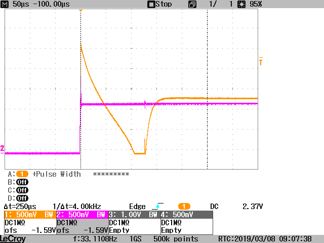
I'm seeing transients that I can't fully explain when the set of three devices is enabled. It looks like the amplifier is saturating, taking approximately 150us, and finally recovering and returning to expected behavior. I've done lots of simulations, and have found that I can replicate the result in simulations by adding imbalance to the capacitors on the load cell lines so that the amplifier saturates. I also tried adding this imbalance to the hardware, but it didn't seem to affect the amplifier output.
Next, I tried having the reference always powered, so that only the load cell and amplifier enable were switched on and off - this changed the waveform, but didn't make it any better. Finally, I kept the load cell and reference enabled so that only the amplifier enable was switched, and the output was stable at the appropriate value.
The transients aren't an issue in the application, since I can just wait them out before reading the ADC, but I would like to understand them better so that I can have better confidence in the design.
The image below shows the output of the op amp (orange) and the reference voltage (pink).