This thread has been locked.

If you have a related question, please click the "Ask a related question" button in the top right corner. The newly created question will be automatically linked to this question.

OPA615: Supply rail and Bias problem

Part Number: OPA615
Other Parts Discussed in Thread: OPA860, TINA-TI

I am using the OPA615 as a high speed integrator as per Fig 47 in the data sheet. I have simulated it in Altium and all looks OK. There is something wrong on my board however. When I power up, the -5V line gets dragged down and my chip starts to overheat. I have resolved this by adding a resistor (1Meg) from the base (pin 2) to ground. This appears to work and stops the -5V being dragged down but I am not clear why this is necessary and why it is not shown or mentioned in the DS. The downside of course is that my hold capacitor is discharging quite rapidly. 

Any thoughts?

Ian


  • Hi Ian,

    are you sure the power supply can deliver enough supply current? Is a current limit set accidently?

    How do you connect "hold control"?

    Can you show the results of your simulation? Have you scope plots of your measurements?

    Kai
  • Hello Ian,

    When you say VS- is being dragged down, do you mean it goes to 0V? Are you using the circuit as an integrator for ns pulses? Because if not, you might need a resistor between the Hold control pin to its source.
    Why have you added a 100Ohm Re resistor R115 from emitter/output to ground?

    Thanks!
    -Karan
  • Hi Karan,

    The 100R resistor is a hangover from the simulation and has now been removed but without improvement. The device is used as an integrator as per the DS. The Hold control is directly connected to a DS90LT012 running at 3V3.

    I am running my input pulses through at 10kHz. The circuit has 3 devices connected to the -5V rail, a couple of OPA695s further upstream and the OPA615. In quiescent the circuit draws 35mA on this rail. The moment I connect the pulse train to the input the supply current on the -5V jumps to 136mA and the 615 gets very hot. 

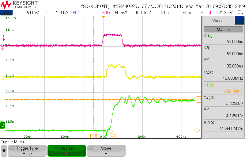
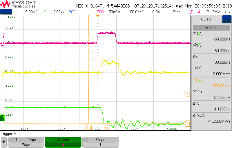
    The magenta is my input pulse to the SH+, the yellow my HOLD pulse and the green my output at pin 1. Sometimes I get a positive integration to ~3.2V and sometimes it resets to -900mV.  


  • Hi Kai,

    The current limit is not set too low. See my comments to Karan about the changes to the current level and HOLD control. The simulation results are shown below for a typical input:


  • I have since disconnected my input the the left of R70. The SH+ input is therefore connected to GND via 150R. I still get similar results even with no input signal.....


    The magenta is my input to GND. The yellow is again my HOLD. The green is the output from pin 1. R115 is removed and the 1M I mentioned in my original post is also removed. It can be seen in the above that the output is different on nearly every pulse. As before, the mean current on the -5V rail jumps to 135mA when the 10kHz input is switched in.      

  • Hi Ian,

    is the OPA615 damaged? Try a fresh one.

    This ns integrator is a bit difficult to use. The feedback network and the input signal must match each other. Have you thought about using a peak detector instead?

    Have you seen these threads?

    e2e.ti.com/.../718099

    e2e.ti.com/.../730231

    Kai
  • Hi again,

    I need an integrator function as sometimes my signals are saturated and integrating this gives me a measure of how saturated they are.

    I have now got a second circuit working which shows some similar and some different issues but seems to be "more working" than the first. Having removed the added 1M resistor from the base of circuit 1 and it appearing to be OK I did the same to the new circuit 2. It immediately went from 38mA on the -5V rail to >100mA. I put a 2.5M resistor back on and the quiescent current went back to normal.

    I now tried changing the pulse width to 40ns as this is the shortest I can get on my sig gen. Circuit 1 would not integrate at all on the output until I reached 100ns width. At that point it went straight to drawing lots of current on -5V. As soon as I dropped the width to 80ns it was OK again. On circuit 2 i did the same but got different results. At 40ns and upwards the output seemed to integrate correctly ans discharged through the 2.5M resistor when in HOLD mode. However like circuit 1, once I went to 100ns width it immediately jumped to high current on -5V. I tried dropping the input signal level by a factor of 2 but had the same result.

    Still puzzled.

    Ian
  • Hi Ian,

    are you exceeding the allowed input voltage range at the OTA base?

    Kai
  • I appear to be hitting the limit from the plots I posted. Surely in integration mode, this CHOLD output will integrate to whatever the circuit dictates? Are you suggesting there is some mechanism internally which possibly puts some internal diode or transistor into a forward bias condition and soaks up lots of -5V current?
  • The CHOLD output voltage compliance (+/-3.5V typ) is actually slightly greater than the allowed Base input (+/-3.4V typ, +/-3.0V over temp range).
  • Hi Ian,

    I don't get the OPA615 simulation to run. So, I would recommend to use the OPA860, as shown here:

    e2e.ti.com/.../718099

    Kai
  • Hello Kai,

    Thanks. I did look at the OPA860 but I was trying a bit more yet on the OPA615. I found the 615 simulation needed some tweeks to get it to run ok. The droop on the hold output looks quite significant on the plots you posted. I guess this is because there is leakage back into the OTA?

    Ian
  • Hi Ian,

    the OPA860 and OPA615 are wonderfully fast. But when it comes to DC precisison they are not so wonderful. This is especially true, if you operate these chips with small integrating caps and high ohmic feedback loops, which these chips are not orginally designed to work with. They can be used, if anything other OPAmp circuitry fails. But don't be surprised, when offset voltage, input bias currents, etc. create considerable errors and unlinearity. You can see that I added lots of auxiliary circuitry in my simulations to prevent these chips from saturating at the output or generating huge offset voltages. That's the price you have to pay for this outstanding speed...

    While the peak detector is working rather reliably with these chips within a wide range of input signals, the ns integrator can become really really tricky. I already mentioned the huge output bouncing lasting for about 10µs. More, the ns integrator can only work satisfyingly with very certain input signals (shape, duration, amplitude, repeat rate, etc.). Two decades ago I struggled with the ns integrator using the OPA660. I get it to work, but only for a rather unchanging input signal shape. That's why I recommended to use the peak detector instead of ns integrator. :-)

    Do you have a TSC-file for the TINA-TI simulation you could share?

    Kai

  • Hi Kai,

    Thanks for the warning. I shall carry on a bit further yet before looking for another option.

    I have the simulation netlist file from Altium for the circuit I posted earlier.

    See attached.

    Ian

    Receiver Pulse Integrator
    *SPICE Netlist generated by Advanced Sim server on 22-Mar-19 1:53:36 PM
    
    *Schematic Netlist:
    C1 0 Vcap 33p IC=0
    C2 0 NetC2_2 1000n
    E1 NetE1_2 0 VALUE {0.5 * V(NetE1_1)}
    E2 Vout 0 VALUE {4 * V(NetE2_1)}
    R1 Vin NetR1_2 150
    R2 Vcap Vb 100
    R3 0 Vin 50
    R4 NetR4_1 NetR4_2 300
    R5 0 HOLD 50
    R6 NetR6_1 NetC2_2 820
    R7 NetC2_2 NetR7_2 820
    R8 NetR7_2 NetE2_1 50
    R9 0 NetE2_1 50
    R10 0 Vout 1000
    R101 0 NetR101_2 1000
    XU1 Vb 0 Vcap NetR7_2 0 HOLD NetR4_2 NetR1_2 NetR6_1 NetU1_13 NetR4_1 OPA615_model
    AU2 NetE1_2 Vin AU2LIMIT
    .MODEL AU2LIMIT limit (  out_lower_limit=0 out_upper_limit=3.5  )
    V1 NetR101_2 0 DC 0 PWL(10n 0V 10.395n 0.016 10.767n .077 10.976n .159 11.162n
    + .267 11.371n .418 11.603n .59 11.975n .751 12.416n .932 12.672n .979 12.881n 1
    + 13.183n .971 13.555n .87 13.903n .743 14.182n .61 14.786n .407 15.390n .275
    + 16.157n .165 17.342n .094 18.620n .059 20.711n .033 21.849n .013 22.803n 0) AC 1
    + 10n
    V2 0 NetR4_1 5
    V3 HOLD 0 DC 0 PULSE(0 5 9n 1n 1n 120n 100u) AC 1 0
    V4 NetU1_13 0 5
    V5 NetE1_1 0 DC 0 PULSE(0 5 9n 1n 1n 120n 100u) AC 1 0
    
    .SAVE 0 HOLD NetC2_2 NetE1_1 NetE1_2 NetE2_1 NetR1_2 NetR101_2 NetR4_1 NetR4_2
    .SAVE NetR6_1 NetR7_2 NetU1_13 Vb Vcap Vin Vout V1#branch V2#branch V3#branch
    .SAVE V4#branch V5#branch @V1[z] @V2[z] @V3[z] @V4[z] @V5[z] @C1[i] @C2[i] @R1[i]
    .SAVE @R10[i] @R101[i] @R2[i] @R3[i] @R4[i] @R5[i] @R6[i] @R7[i] @R8[i] @R9[i] @C1[p]
    .SAVE @C2[p] @E1[p] @E2[p] @R1[p] @R10[p] @R101[p] @R2[p] @R3[p] @R4[p] @R5[p] @R6[p]
    .SAVE @R7[p] @R8[p] @R9[p] @V1[p] @V2[p] @V3[p] @V4[p] @V5[p]
    
    *PLOT TRAN -1 1 A=HOLD A=Vb A=Vin A=Vout
    *PLOT OP -1 1 A=HOLD A=Vb A=Vin A=Vout
    
    .OPTION KeepLastSetup=False
    .OPTIONS ITL1=400 METHOD=GEAR MAXORD=3
    *Selected Circuit Analyses:
    .TRAN 1E-11 2E-7 0 1E-8 UIC
    .OP
    
    *Models and Subcircuits:
    .SUBCKT OPA615_model B C C_Hold E Gnd Hold_Ctrl IqAdj S_H_InP S_H_InM Vcc Vee
    .PARAM x1 = 0.125
    .PARAM x2 = {x1*2}
    .PARAM x3 = {x1*3}
    .PARAM x4 = {x1*4}
    .PARAM x8 = {x1*8}
    .PARAM x10 = {x1*10}
    .PARAM x12 = {x1*12}
    .PARAM x20 = {x10*2}
    .PARAM x40 = {x10*4}
    .PARAM x80 = {x40*2}
    R_U1_U2_R12         N_0002 N_0001  100
    Q_U1_U2_Q9         N_0004 N_0003 N_0005 NPN8 {x8}
    R_U1_U2_R13         N_0006 N_0002  100
    Q_U1_U2_Q12         N_0006 N_0007 N_0008 NPN8 {x2}
    Q_U1_U2_Q13         N_0007 N_0007 N_0008 NPN8 {x2}
    Q_U1_U2_Q1         N_0004 N_0059 Vmid NPN8 {x3}
    Q_U1_U2_Q4         N_0009 N_0004 N_0010 PNP8 {x8}
    Q_U1_U2_Q6         N_0001 N_0003 N_0011 PNP8 {x2}
    Q_U1_U2_Q5         N_0004 N_0004 N_0012 PNP8 {x10}
    Q_U1_U2_Q15         N_0013 N_0013 N_0014 NPN8 {x10}
    Q_U1_U2_Q17         N_0013 N_0007 N_0015 PNP8 {x8}
    Q_U1_U2_Q16         N_0016 N_0013 N_0017 NPN8
    Q_U1_U2_Q7         N_0003 N_0003 N_0011 PNP8 {x2}
    Q_U1_U2_Q21         N_0019 N_0018 N_0020 PNP8 {x4}
    Q_U1_U2_Q2         N_0013 N_0061 Vmid PNP8 {x3}
    Q_U1_U2_Q10         N_0015 N_0002 N_0021 PNP8 {x8}
    Q_U1_U2_Q8         N_0009 N_0009 N_0021 NPN8 {x2}
    Q_U1_U2_Q18         N_0016 N_0016 N_0022 PNP8 {x2}
    Q_U1_U2_Q11         N_0005 N_0002 N_0022 NPN8 {x8}
    Q_U1_U2_Q23         N_0022 N_0023 N_0021 PNP8 {x8}
    Q_U1_U2_Q24         N_0021 N_0023 N_0022 NPN8 {x8}
    Q_U1_U2_Q20         N_0020 N_0018 N_0019 NPN8 {x4}
    Q_U1_U2_Q26         N_0024 N_0020 N_0025 NPN8 {x40}
    R_U1_U2_R22         E N_0025  3
    R_U1_U2_R23         N_0026 E  3
    Q_U1_U2_Q25         N_0027 N_0019 N_0026 PNP8 {x40}
    Q_U1_U2_Q31         N_0027 N_0027 N_0028 NPN8 {x80}
    Q_U1_U2_Q32         N_0029 N_0027 N_0030 NPN8 {x80}
    Q_U1_U2_Q34         N_0031 N_0031 N_0032 NPN8 {x1}
    Q_U1_U2_Q37         N_0031 N_0031 N_0033 PNP8 {x1}
    R_U1_U2_R24         Vee N_0028  12
    Q_U1_U2_Q14         N_0008 N_0008 Vee NPN8 {x2}
    R_U1_U2_R14         Vee N_0017  125
    R_U1_U2_R17         Vee N_0014  100
    Q_U1_U2_Q22         Vee N_0016 N_0019 PNP8 {x4}
    R_U1_U2_R25         Vee N_0030  12
    R_U1_U2_R27         Vee N_0034  4k
    Q_U1_U2_Q36         N_0035 N_0035 N_0032 PNP8 {x1}
    Q_U1_U2_Q30         C N_0036 N_0029 NPN8 {x40}
    Q_U1_U2_Q42         Vee N_0037 N_0036 PNP8 {x2}
    Q_U1_U2_Q38         N_0037 N_0037 N_0034 NPN8 {x1}
    Q_U1_U2_Q3         N_0011 N_0011 Vcc PNP8 {x2}
    R_U1_U2_R15         N_0012 Vcc  100
    R_U1_U2_R16         N_0010 Vcc  125
    Q_U1_U2_Q19         Vcc N_0009 N_0020 NPN8 {x4}
    R_U1_U2_R21         N_0038 Vcc  12
    R_U1_U2_R26         N_0033 Vcc  4k
    Q_U1_U2_Q40         Vcc N_0039 N_0036 NPN8 {x2}
    Q_U1_U2_Q39         N_0039 N_0039 N_0040 NPN8 {x1}
    Q_U1_U2_Q41         N_0037 N_0037 N_0040 PNP8 {x1}
    G_U1_U2_G1         Vcc N_0039 N_0057 N_0041 1.03103782735
    G_U1_U2_G2         N_0035 Vee N_0053 N_0041 1.01910219675
    E_U1_U2_E1         N_0041 Vee Vcc Vee 0.5
    Q_U1_U2_Q29         C N_0042 N_0043 PNP8 {x40}
    Q_U1_U2_Q33         Vcc N_0031 N_0042 NPN8 {x2}
    Q_U1_U2_Q35         Vee N_0035 N_0042 PNP8 {x2}
    R_U1_U2_R20         N_0044 Vcc  12
    Q_U1_U2_Q45         N_0043 N_0024 N_0038 PNP8 {x80}
    Q_U1_U2_Q44         N_0024 N_0024 N_0044 PNP8 {x80}
    R_U1_U2_R11         B N_0002  400
    X_U1_U3_H1    N_0045 N_0046 N_0093 Vmid OPA615_Model_U1_U3_H1
    X_U1_U3_F1    N_0046 N_0047 Vcc N_0048 OPA615_Model_U1_U3_F1
    R_U1_U3_R18         N_0049 IqAdj  50
    R_U1_U3_R16         N_0049 N_0050  750
    X_U1_U3_H3    N_0051 N_0052 N_0053 Vmid OPA615_Model_U1_U3_H3
    X_U1_U3_F2    N_0054 N_0050 N_0055 N_0056 OPA615_Model_U1_U3_F2
    X_U1_U3_H4    Vcc N_0055 N_0057 Vmid OPA615_Model_U1_U3_H4
    X_U1_U3_F5    N_0056 N_0051 Vcc N_0058 OPA615_Model_U1_U3_F5
    Q_U1_U3_Q1         N_0058 N_0059 Vmid NPN8 {x1}
    Q_U1_U3_Q2         Vcc N_0058 N_0059 NPN8 {x1}
    Q_U1_U3_Q3         N_0059 N_0059 Vmid NPN8 {x1}
    X_U1_U3_F4    N_0052 Vee N_0060 Vee OPA615_Model_U1_U3_F4
    E_U1_U3_E2         Vmid Vee Vcc Vee 0.5
    V_U1_U3_V2         N_0045 Vee DC 0.11145V
    R_U1_U3_R11         Vee N_0047  750
    R_U1_U3_R15         Vee Vcc  57.8369k
    R_U1_U3_R17         Vee N_0049  50k
    V_U1_U3_V3         N_0054 Vee DC 0.113159160873V
    Q_U1_U3_Q5         N_0061 N_0061 Vmid PNP8 {x1}
    Q_U1_U3_Q6         Vee N_0060 N_0061 PNP8 {x1}
    Q_U1_U3_Q4         N_0060 N_0061 Vmid PNP8 {x1}
    X_U1_U3_H2    N_0048 Vee Vmid N_0104 OPA615_Model_U1_U3_H2
    R_U1_U4_R14         S_H_InM N_0062  50
    Q_U1_U4_Q6         e_dn Lgc_L N_0063 PNP8 {x1}
    Q_U1_U4_Q8         e_up N_0102 N_0064 NPN8 {x1}
    G_U1_U4_G1         Vcc N_0065 N_0093 Vmid2 1.39502018843
    Q_U1_U4_Q2         Vcc N_0062 N_0066 NPN8 {x2}
    Q_U1_U4_Q3         Vcc N_0065 N_0067 NPN8 {x12}
    Q_U1_U4_Q7         Vcc Lgc_L N_0064 NPN8 {x1}
    R_U1_U4_R23         N_0068 S_H_InP  50
    Q_U1_U4_Q12         Vcc N_0068 N_0069 NPN8 {x2}
    Q_U1_U4_Q11         N_0071 N_0070 N_0067 NPN8 {x12}
    Q_U1_U4_Q17         C_Hold N_0089 N_0072 PNP8 {x40}
    Q_U1_U4_Q13         N_0071 N_0071 Vcc PNP8 {x10}
    Q_U1_U4_Q18         Vee N_0091 N_0072 PNP8 {x20}
    G_U1_U4_G2         N_0066 Vee Vmid2 N_0104 1.24029451138
    E_U1_U4_E1         Vmid2 Vee Vcc Vee 0.5
    Q_U1_U4_Q4         Vee N_0066 N_0067 PNP8 {x12}
    Q_U1_U4_Q1         Vee N_0062 N_0065 PNP8 {x2}
    Q_U1_U4_Q5         Vee N_0102 N_0063 PNP8 {x1}
    Q_U1_U4_Q9         Vee N_0068 N_0070 PNP8 {x2}
    Q_U1_U4_Q15         N_0073 N_0073 Vee NPN8 {x10}
    Q_U1_U4_Q19         C_Hold N_0094 N_0074 NPN8
    G_U1_U4_G8         N_0069 e_dn Vmid2 N_0104 1.34
    G_U1_U4_G6         e_up N_0070 N_0093 Vmid2 1.382
    Q_U1_U4_Q16         N_0074 N_0073 Vee NPN8 {x10*1.02}
    Q_U1_U4_Q14         N_0072 N_0071 Vcc PNP8 {x10*1.02}
    Q_U1_U4_Q20         Vcc N_0095 N_0074 NPN8
    V_U1_U4_V5         e_up Vcc DC -353m
    V_U1_U4_V6         e_dn Vee DC 313.5m
    G_U1_U4_G4         Vcc N_0063 N_0093 Vmid2 3.46567967699
    G_U1_U4_G5         N_0064 Vee Vmid2 N_0104 3.07228915663
    Q_U1_U4_Q10         N_0073 N_0069 N_0067 PNP8 {x12}
    G_U1_U4_G7         Vcc N_0073 N_0093 Vmid2 0.80215
    G_U1_U4_G9         N_0071 Vee Vmid2 N_0104 1.1
    D_U1_U5_D1         N_0075 N_0076 DX
    D_U1_U5_D3         N_0077 N_0078 DX
    Q_U1_U5_Q2         N_0080 N_0079 N_0081 PNP8 {x2}
    R_U1_U5_R16         N_0077 N_0079  3k
    R_U1_U5_R17         N_0083 N_0082  1.5k
    R_U1_U5_R18         N_0083 N_0084  1.5k
    V_U1_U5_V1         N_0083 Vee 2.4V
    Q_U1_U5_Q6         N_0084 Lgc_L N_0085 PNP8 {x2}
    R_U1_U5_R20         N_0087 N_0086  1.5k
    R_U1_U5_R19         N_0088 N_0086  1.5k
    Q_U1_U5_Q9         Vee N_0088 N_0089 PNP8 {x1}
    Q_U1_U5_Q12         N_0087 Lgc_H N_0090 NPN8
    Q_U1_U5_Q11         N_0088 Lgc_L N_0090 NPN8
    Q_U1_U5_Q10         Vee N_0087 N_0091 PNP8 {x1}
    Q_U1_U5_Q1         N_0092 N_0075 N_0081 PNP8 {x2}
    C_U1_U5_C1         Gnd N_0079  2p
    D_U1_U5_D2         Gnd N_0076 DX
    R_U1_U5_R15         Gnd N_0080  1.5k
    R_U1_U5_R14         Gnd N_0092  1.5k
    Q_U1_U5_Q3         Gnd N_0079 N_0075 PNP8 {x2}
    Q_U1_U5_Q4         N_0078 N_0078 Gnd NPN8 {x1}
    Q_U1_U5_Q5         N_0082 Lgc_H N_0085 PNP8 {x2}
    G_U1_U5_G3         Vcc N_0079 N_0093 Vmid 0.995962314939
    G_U1_U5_G2         Vcc N_0081 N_0093 Vmid 1.97039030956
    G_U1_U5_G1         Vcc N_0075 N_0093 Vmid 0.993943472409
    G_U1_U5_G4         Vcc N_0085 N_0093 Vmid 1.97913862719
    Q_U1_U5_Q7         Vcc N_0082 N_0094 NPN8 {x1}
    Q_U1_U5_Q8         Vcc N_0084 N_0095 NPN8 {x1}
    G_U1_U5_G5         Vcc N_0096 N_0093 Vmid 1.9663526245
    E_U1_U5_E1         Vmid N_0097 Vcc N_0097 0.5
    G_U1_U5_G6         Vcc N_0098 N_0093 Vmid 1.9663526245
    V_U1_U5_V4         Vcc N_0086 DC 2.4V
    V_U1_U5_V6         N_0098 N_0091 DC 0
    V_U1_U5_V5         N_0096 N_0089 DC 0
    V_U1_U5_V7         N_0092 N_0099
    V_U1_U5_V8         N_0080 Lgc_L
    V_U1_U5_V9         Lgc_L N_0100
    V_U1_U5_V10         N_0099 N_0101
    V_U1_U5_V11         N_0102 N_0099
    V_U1_U5_V12         N_0099 Lgc_H
    V_U1_U5_V13         N_0090 N_0103
    G_U1_U5_G11         N_0103 Vee N_0104 Vmid -1.98259705489
    G_U1_U5_G10         N_0095 Vee N_0104 Vmid -1.97389558233
    G_U1_U5_G9         N_0094 Vee N_0104 Vmid -1.97590361446
    G_U1_U5_G8         N_0100 Vee N_0104 Vmid -1.00066934404
    G_U1_U5_G7         N_0101 Vee N_0104 Vmid -1.00066934404
    R_U1_U5_R25         Hold_Ctrl N_0076  500
    .MODEL NPN8 NPN IS = 7.604E-18 BF = 1.570E+02 NF = 1.000E+00 VAF= 7.871E+01 IKF=
    + 3.975E-02 ISE= 3.219E-14 NE = 2.000E+00 BR = 7.614E-01 NR = 1.000E+00 VAR=
    + 1.452E+00 IKR= 8.172E-02 ISC= 7.618E-21 NC = 1.847E+00 RB = 1.060E+02 IRB=
    + 0.000E+00 RBM= 2.400E+00 RE = 2.520E+00 RC = 1.270E+02 CJE= 1.120E-13 VJE=
    + 7.591E-01 MJE= 5.406E-01 TF = 1.213E-11 XTF= 2.049E+00 VTF= 1.813E+00 ITF=
    + 4.293E-02 PTF= 0.000E+00 CJC= 8.208E-14 VJC= 6.666E-01 MJC= 4.509E-01
    + XCJC=8.450E-02 TR = 4.000E-11 CJS= 1.160E-13 VJS= 5.286E-01 MJS= 4.389E-01 XTB=
    + 1.022E+00 EG = 1.120E+00 XTI= 1.780E+00 KF = 3.500E-16 AF = 1.000E+00 FC =
    + 8.273E-01
    .MODEL PNP8 PNP IS = 7.999E-18 BF = 1.418E+02 NF = 1.000E+00 VAF= 4.158E+01 IKF=
    + 1.085E-01 ISE= 2.233E-15 NE = 1.505E+00 BR = 3.252E+01 NR = 1.050E+00 VAR=
    + 1.093E+00 IKR= 5.000E-05 ISC= 6.621E-16 NC = 1.150E+00 RB = 6.246E+01 IRB=
    + 0.000E+00 RBM= 2.240E+00 RE = 2.537E+00 RC = 1.260E+02 CJE= 9.502E-14 VJE=
    + 7.320E-01 MJE= 4.930E-01 TF = 1.303E-11 XTF= 3.500E+01 VTF= 3.259E+00 ITF=
    + 2.639E-01 PTF= 0.000E+00 CJC= 1.080E-13 VJC= 7.743E-01 MJC= 5.000E-01
    + XCJC=8.504E-02 TR = 1.500E-10 CJS= 1.290E-13 VJS= 9.058E-01 MJS= 4.931E-01 XTB=
    + 1.732E+00 EG = 1.120E+00 XTI= 2.000E+00 KF = 3.500E-16 AF = 1.000E+00 FC =
    + 8.500E-01
    .MODEL DX D IS=1.0000E-15
    .ENDS OPA615_model
    
    .subckt OPA615_Model_U1_U3_H1 1 2 3 4
    H_U1_U3_H1         3 4 VH_U1_U3_H1 1
    VH_U1_U3_H1         1 2 0V
    .ENDS OPA615_Model_U1_U3_H1
    
    .subckt OPA615_Model_U1_U3_F1 1 2 3 4
    F_U1_U3_F1         3 4 VF_U1_U3_F1 1.00538358008
    VF_U1_U3_F1         1 2 0V
    .ENDS OPA615_Model_U1_U3_F1
    
    .subckt OPA615_Model_U1_U3_H3 1 2 3 4
    H_U1_U3_H3         3 4 VH_U1_U3_H3 1
    VH_U1_U3_H3         1 2 0V
    .ENDS OPA615_Model_U1_U3_H3
    
    .subckt OPA615_Model_U1_U3_F2 1 2 3 4
    F_U1_U3_F2         3 4 VF_U1_U3_F2 1.01551891368
    VF_U1_U3_F2         1 2 0V
    .ENDS OPA615_Model_U1_U3_F2
    
    .subckt OPA615_Model_U1_U3_H4 1 2 3 4
    H_U1_U3_H4         3 4 VH_U1_U3_H4 1
    VH_U1_U3_H4         1 2 0V
    .ENDS OPA615_Model_U1_U3_H4
    
    .subckt OPA615_Model_U1_U3_F5 1 2 3 4
    F_U1_U3_F5         3 4 VF_U1_U3_F5 1
    VF_U1_U3_F5         1 2 0V
    .ENDS OPA615_Model_U1_U3_F5
    
    .subckt OPA615_Model_U1_U3_F4 1 2 3 4
    F_U1_U3_F4         3 4 VF_U1_U3_F4 1
    VF_U1_U3_F4         1 2 0V
    .ENDS OPA615_Model_U1_U3_F4
    
    .subckt OPA615_Model_U1_U3_H2 1 2 3 4
    H_U1_U3_H2         3 4 VH_U1_U3_H2 1
    VH_U1_U3_H2         1 2 0V
    .ends OPA615_Model_U1_U3_H2
    
    .END
    

  • Also, My plan is to use the integrator to capture my signal but then to feed it to an ADC and sample the integrated signal close to its peak (within 0.5-1us).
  • Good luck!

    Kai