This thread has been locked.

If you have a related question, please click the "Ask a related question" button in the top right corner. The newly created question will be automatically linked to this question.

INA200: Pin No 2 (Amplifier OUT) is high at all Rising edge of output pulse even at No-Load

Part Number: INA200

Dear Team,

It's the 2nd time i am posting in forum. Thanks in advance for your previous & upcoming strong  technical support.

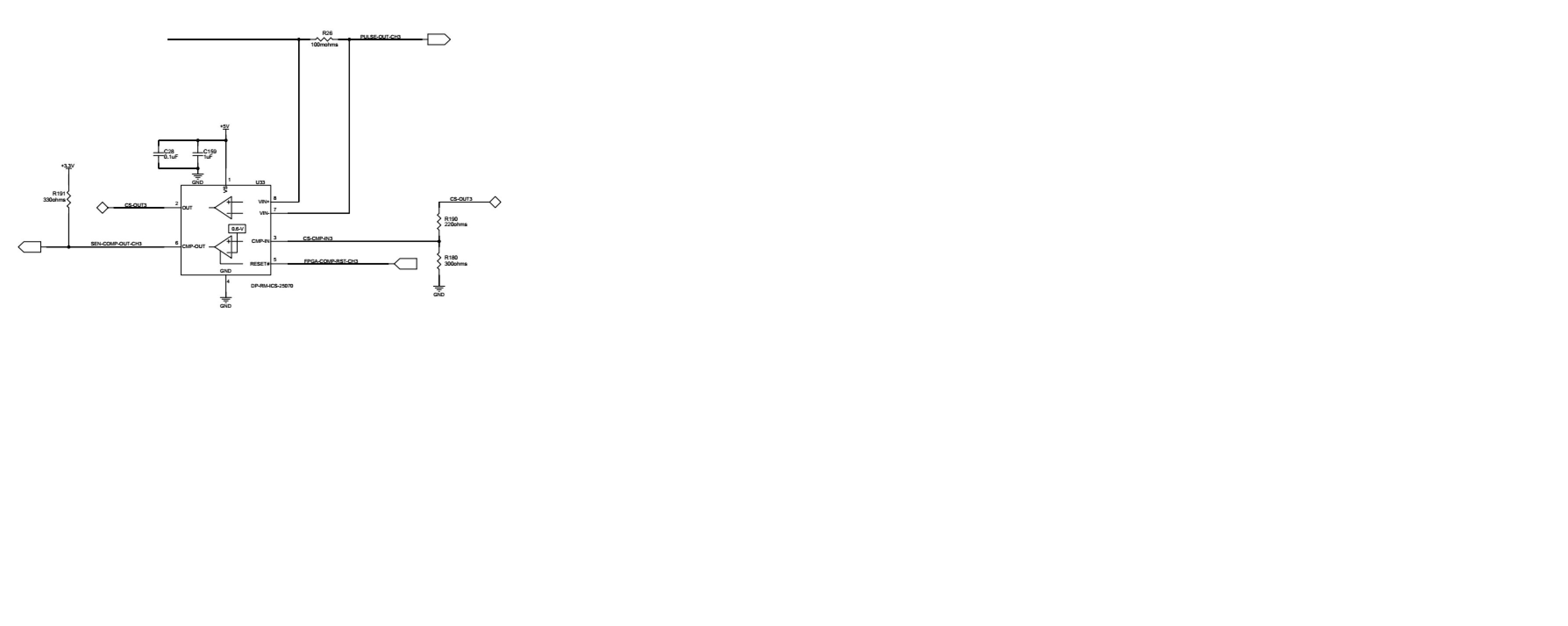
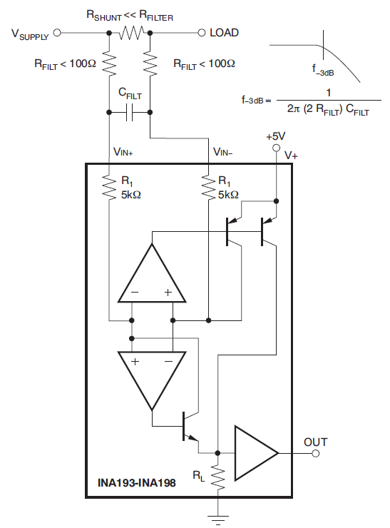
INA200AIDGKT IC is being used in a over-current sensing & protection application(Schematics attached). Output voltage is not a continuous one  but a pulsed one.Details of pulse is mentioned below:

ON Time : 1.5mS; OFF Time : 98.5mS; Voltage Amplitude: 2.5V to 40V; Load current : 100mA(constant load); Over-current limit : 500mA.

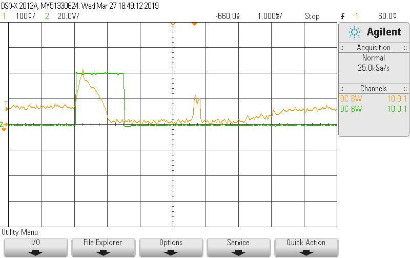
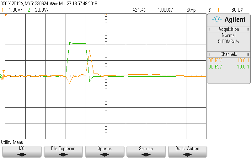
So the duty of INA200 IC is clearly to disable the gate driver whenever load current crosses 500mA; I mean only when the load current through sense resistor goes beyond 500mA, Comparator must go high.But interestingly during testing i found that the out pin of amplifier goes high at all the rising edges of the output  pulse even though output is at no load condition. And sometimes this causes the comparator output to go high (false trigger). Scopeshotsattached for your reference.

Awaiting for your reply.

Regards,

Devarajan R

  • In continuation to previous one

    Scopeshot 1 is captured for pulse of ON Time 1.5mS, OFF time 98.5mS, Voltage 40V & output at no-Load; Scopeshot 2 is captured for pulse of ON Time 1uS , OFF Time 99uS, Voltage 40V & output at No-Load.

    Green is output pulse while yellow is amplifier out.

  • Green is output pulse & Yellow is amplifier out

  • Hello Devarajan,

    Thanks for using the forum. We are always happy to support and solve your engineering problems.

    This seems to me like a problem with AC CMRR. When you say the output is pulsing I assume you mean node “Pulse-Out-CH3” and this is essentially the common-mode voltage (VCM) of INA200. When the VCM changes this induces an input offset voltage into the internal current sense amplifier. Now as this offset changes more rapidly the CMRR begins to degrade. This is shown in Figure 5 of data sheet.

    For this system VCM step is large (40V) and is happening quickly. In your second plot the VCM step could be considered having a frequency of 1MHz and figure 5 implies that CMRR can drop to 50 dB at 1MHz extrapolating with -20dB/decade slope. You can calculate the offset change as 40V* 10^(-50/20) = 126mV. If this is gained up by 20 that turns into 2.53V on the output. Even at 70 dB CMRR (100kHz), the VOUT change is 253mV.

    On top of all of this, the sense voltage at 100mA is 10mV and this is underneath the specified 20mV we characterize the part with. As the data sheet explains, when Vsense < 20mV, the device is not operating linearly anymore and the output can become saturated at 0.4V (when VCM=0V and VS=5V) according to Electrical Characteristics table. This is something to keep in mind.

    The problem could be mitigated by filtering the output with filter before the comparator.

    Sincerely,
    Peter
  • Hello Peter,

    Thanks for your reply.

    I tried with pulse period of 10mS (100Hz) & voltage of 40V. In that i could find the IC functioning as per theory.

    As per your reply, CMR depends only on total time of pulse (Time=1/Frequency) & voltage magnitude. But while reducing the ON time of pulse to 1uS with same frequency (100Hz) & voltage (40V), ic again misbehaves. I mean at no-load i found some pulse in amplifier output. Why does it depend on ON Time of pulse?.

    Regards,

    Devarajan R

  • Hey Devarajan,

    The total ON time of the pulse should have less to do with the CMR when compared to the effects due to the actual rise/fall times of the pulse. What is actually generating the output offset is the quick voltage step of VCM, not the ON time. If the VCM was to ramp much more slowly with a rise time of a few milliseconds, then the internal amplifier would have time to correct any changes in the input offset (Vos) and thus no glitches on the output; however, in your initial plots, the rise times are ~25us and ~200ns respectively. This quick rise in VCM can be considered the partial zoom-in of a continuous sine-wave with a frequency much faster than frequency of the actual pulse.

    I could see that when you decrease the ON time enough, there could be a compounding effect in the output offset since you have two large VCM steps occurring very close to each other. Before the output has time to settle from 0V to 40V step, the input is driven from 40V to 0V quickly. When you increase the ON time you put time in between these rise and fall times and thus give time for the output to settle before being bombarded with the step down VCM.

    Another option is to place a filter at the inputs of INA200 for example capacitors from IN+ and IN- to ground that would dampen the VCM step and thus slow down the rise time, although this of course will add capacitance to your load and this might not be possible in your system. Adding some current-limiting resistance on the input traces would help reduce the instantaneous current needed to charge the capacitors for every 40V step, but these resistors add error and this is discussed in section 7.4.1 of datasheet.

    Sincerely,
    Peter Iliya
    Current Sensing Applications
  • Dear Sir,

    From your reply & testing observations, I could understand that for proper operation of IC (as per theory),  i should  reduce the  voltage level. While testing at 10V, i observed that voltage at CS out pin is at 0V; While at higher voltages (say 20V, 30V & 40V) the voltage at CS out pin is risen from 0V. And i could understand this rise is due to incapability of op-amp to reject CM noise at specific voltage & frequency.

    So finally i thought of using a potential divider circuit to reduce the voltage at V= & V- pin. I mean, when pulse out voltage is 40V, at V+ & V- pins it will be 10V. So maximum input voltage for the  IC is limited to 10V and i hope the IC could work well with good CMR. Kindly suggest if there is some other problem in using potential divider at the input pins.  

    Also request you to clarify, is there any maximum limit for sense voltage level at V+ & V- pins.

    Regards,

    Devarajan R

  • Also can you please elaborate the formula used to calculate offset due to common mode pulse. I could understood that you have calculated CMRR from given CMR using 10^(dB/20) and then multiplying the this CMR value with Input Voltage (say 40V in my case). But i could not understand why do u multiply the input voltage with CMRR.

    What i learnt so far is, from CMRR & Differential gain of op-amp, we can calculate CM gain using formula CMRR =AD / ACM. And then by multiplying this ACM with input CM voltage we get offset in output due to CM voltage in input. While thinking from this aspect your formula seems a bit confused. Can u pl. help me in this regard?

    Regards
    Devarajan R
  • Devarajan,

    Using two resistor-dividers at each input pin of the device (VIN+, VIN-) is not a good idea. Not only will this load down your source power, but you will also generate significant error at with your Vsense. Even if the resistors are perfectly matched, the mismatch in IB+ and IB- currents will generate a net differential voltage offset and this will severely impact the true shunt voltage you are trying to sense. If you make the resistors larger in value you will reduce the power loss from your bus voltage, but you will dramatically increase input offset error. We usually recommend for many of these devices that you limit the input resistors to 10Ω. For this device the datasheet recommends limiting the resistors to 100Ω as discussed in section 7.4.1. Note that for this device there are 5kΩ (±30%) resistors from the input pins to in actual inputs of internal amplifier.


    The maximum sense (differential) voltage at VIN+ and VIN- is +-18V. This is seen in the Absolute Maximum Ratings Table, Section 6.1. This is the maximum voltage you can have before possibly damaging the device.

    I can elaborate on how I calculated offset due to CMR. CMRR can be expressed as micro-Volts/Volts (µV/V) or by dB. DC CMRR is what you described with ∆differential/∆common-mode. This is characterized by sweeping VCM and measuring Vdiff. The slope of this line is CMRR expressed as µV/V. Thus, if you want to calculate your offset with a range of VCM, use the equation: Vos_cmrr = offset = CMRR*(VCM1 – VCM2) = CMRR*(40V-0V).

    AC CMRR is when you input a sinusoidal VCM and vary the frequency. As you vary the frequency you measure Vdiff and calculate the dB at that specific frequency as CMRR = 20*LOG(-Vdiff/VCM). To calculate offset due to VCM, use the equation: Vos_cmrr = 10^(-CMRR/20)*(VCM_peak-to-peak) = 10^(-50dB/20)*40V for VCM frequency of 1MHz.

    There is essentially no difference in how I calculated Vos_CMRR and how you explained it earlier and the equations used to calculate offset due to CMRR is same for op amps as it is for current sense amplifiers.

    Sincerely,
    Peter Iliya
    Current Sensing Applications