This thread has been locked.

If you have a related question, please click the "Ask a related question" button in the top right corner. The newly created question will be automatically linked to this question.

TL3472: It breaks down when it's powered on

Part Number: TL3472

Dear all:

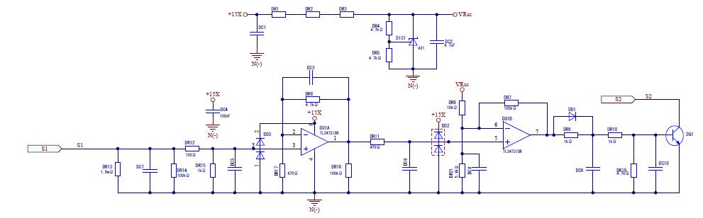
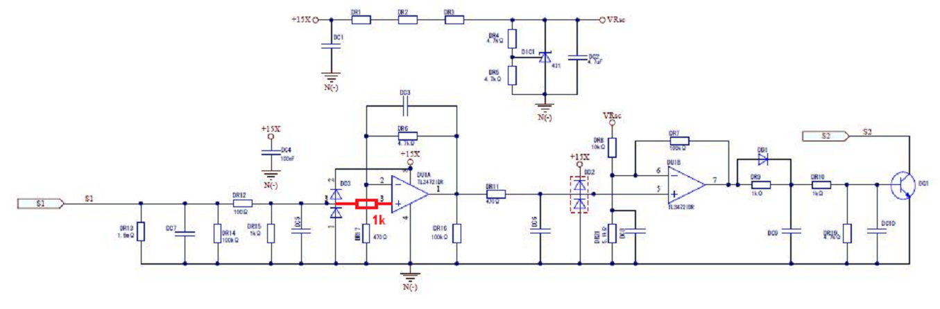
      We have used TL3472 op amp to make frequency converter products. At present, it is found that 5 boards are damaged when TL3472 is powered on.The circuit diagram is as follows.

Under normal circumstances, when S1 is 0V, the first leg of TL3472 is also 0V.But now we have 5 plates, S1 is 0V, TL3472 first leg 5 v.After replacing TL3472, the first pin output 0V is normal.

Please help me check whether there are any defects in my schematic diagram.Or can you give me some Suggestions for change

Thank you!

  • Hello Timsen,

    I expect S1 is subject to ESD, electrostatic discharge. I see some protective elements are already implemented. What is the diode, D03, part number or type of diode? Schottky is prefered. Increasing DR12, DR13 should be helpful, resize DC5 as needed to preserve timing.

    Can you measure the voltages on pins 2 and 3 when S1 is zero and pin 1 is 5V?
    Is the failure symptom always the same?
  • Hi Timsen,

    pin 3 of TL3472 isn't protected enough against input voltages which exceed the supply rails. I would increase DR12. And you could insert an additional resistance between DO3 and pin 3. Remember that only less than 1mA is allowed to flow into pin 3.

    DC4 should directly sit across the supply terminals of TL3472. You can also put a 18V TVS across the supply terminals. And I would mount a TVS directly across the S1 input.

    Kai
  • Hi Ron:
    The same,now we have 5 PCS, S1 is 0V, TL3472 first leg 5 v.After replacing TL3472, the first pin output 0V is normal.Whether pin 1 is a normal 0V or a bad chip output 0V, the voltage on pins 2 and 3 is about 0V。What caused the damage?
  • Hi Timsen,

    have you made the changes which Ron and I have recommended?

    Kai
  • Hi
    (1) this circuit collects the current through the low-resistance precision current detection resistor DR13, which is filtered by RC for the first time, and then sent to DU1A for in-phase amplification, and then output to DU1B for signal comparison.
    (2) your suggestion in the email mentioned that DR12 and DR13 should be increased;As DR13 is our current detection resistance, the resistance value is currently 1.5 milliohm, which cannot be changed according to the design requirements. In the application of higher power, the DR13 resistance value needs to be smaller.
    (3) since DR12 and DC5 constitute the RC filter circuit of the first level, due to the circuit response time requirements, DR12=100 ohms and DC5=10nF, the design requires a time constant within 1us;
    (4) the current DD3 diode is the schottky diode, type 1SS396(TOSHIBA).
    Therefore, the content of your email Suggestions seems to be in conflict with our design. In addition, please provide other Suggestions.
    Thank you!
  • Hi Timsen,

    you could increase DR12 and DR15 by the same factor and decrease DC5 also by this factor. Then neither the division factor nor the time constant is changed. Increasing DR12 to 1k, DR15 to 10k and decreasing DC5 to 1nF is recommended.

    You should also insert this resistor:

    It keeps the current flowing into the TL3472 under 1mA. This is important. Otherwise you violate the absolute maximum ratings. See page 3 of datasheet of TL3472.

    Kai

  • Timsen,

    As Kai said, increasing resistance and changing the capacitance will preserve the response. The red 1k resistor is also very helpful because the current flow through the diode will be more; less current will flow through the op amp input. Without the resistor the spilt would be closer to 50/50 for negative input voltage.
  • Hi Ron/kai:
    S1 signals only VS1 < 1.5 m Ω * 1 A = 1.5 mV, currently DR12 = 100 Ω,
    So into the current TL3472 pin 3 is only to I = 1.5 mV / 100 Ω = 0.015 mA is far less than 1 mA, does not violate the absolute highest rating.
    Your assessment method is different from mine?If not, please list the calculation process for our reference
    Thank you!
  • Timsen,

    I'm not worried about the micros amps and the millivolts. I'm more concerned about ESD, electrostatic discharge. I expect S1 node leaves the board on a connector / wire that could be subject to ESD events.
  • Hi Timsen,

    I agree with Ron. In an industrial environment you have to consider ESD, Surge and Burst. So, hundreds and thousands of volts with varying energies and powers can hit the input of your circuit! In any case you will need a robust input filtering and protection scheme at the input of your circuit.

    Kai