This thread has been locked.

If you have a related question, please click the "Ask a related question" button in the top right corner. The newly created question will be automatically linked to this question.

INA282: Application Question Consultation

Part Number: INA282

Hi,

    I have some questions about INA282 application:

Supplement the customer application scenario: when the current is from left to right,
To output a high level (greater than 1V);
When the current is 0A and is from right to left,
To output a 0V voltage or a voltage less than 0.5V; used to solve the current backflow of the PMOS tube.

1. What is the range of differential voltage values across the sampling resistor?
2. What is the GAIN gain value to do?
3. What is the calculation formula for the sampling current and output voltage?
4. If the unidirectional current is connected from left to right, what state of the output voltage is when the current is from right to left in actual use, and what state will be if the detection current is 0. ?

thanks.

  • Hello Wu,

    Thanks for posting to the forum.

    1. The range of input differential voltages (Full-scale range, or FSR) is limited by the supply voltage (VS) given to the part and the devices gain. So the maximum FSR = VS/Gain = Vsense_max. We define Vsense as (VIN+) - (VIN-), which happens when current flows left to right and is delivered to the load.

    2,3,4. The GAIN value simply multiplies Vsense by gain. So the general equation for VOUT is:

    VOUT = Vsense*GAIN + VREF.

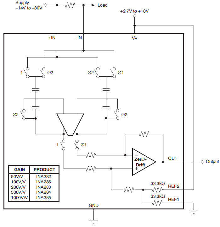
    There are multiple ways to set VREF with INA282 and the internal 33.3kOhm divider provides the benefit of generating a mid-scale reference voltage without external circuitry. So in the picture you have posted, the INA282 is configured with a split-supply reference voltage so VREF = VS/2. This is usually the case when current is symmetrical about 0A and is also demonstrated in sections 7.4.1.2.2 of datasheet, but this does not seem to be the case you have described. Engineer's current is asymmetrical about some point that is not explained in the post.

    Anyway, if you want VOUT = 0.5V, when sense current (Isense) is 0A, then you want VREF=0.5V. This means you will need to drive both REF2 and REF1 pins with a low-output impedance (buffered) 500mV source. Figure 35 in datasheet shows this:

    Customer could just set VREF = VS/2 as shown in first figure to save a component and cost, but they would lose dynamic range. Assuming customer powers INA282 with VS=5V and VREF=2.5V, VOUT would probably never go below 2V if customer is only measuring a small negative current. Its possible this is completely acceptable if customers current range not large.

    Hope this helps. Please consider directing customer to our online training video that explain all of this and much more.

    https://training.ti.com/getting-started-current-sense-amplifiers-session-4-how-choose-appropriate-shunt-resistor?cu=456802

    Sincerely,

    Peter Iliya