This thread has been locked.

If you have a related question, please click the "Ask a related question" button in the top right corner. The newly created question will be automatically linked to this question.

INA3221: Unable to read device registers when A0 is connected to SDA

Part Number: INA3221
Other Parts Discussed in Thread: TCA9406, INA226, MSP430F5500

Hi,

We are using 3 INA3221's on our platform for bus/shunt voltage measurements. Out of 3, 2 Devices are working fine and giving out correct measurements (For one device A0 is connected to VDD 3.3v and for other device the A0 is connected to GND) both of these devices are connected to supplies between (0.7v to 2v). On the third, only 2 channels are in use ( channel 1 1.8v and channel 2 3.3v) we are unable to read anything from 3rd device. 

The pullup on the I2C lines are 4.7k. Below is schematic 

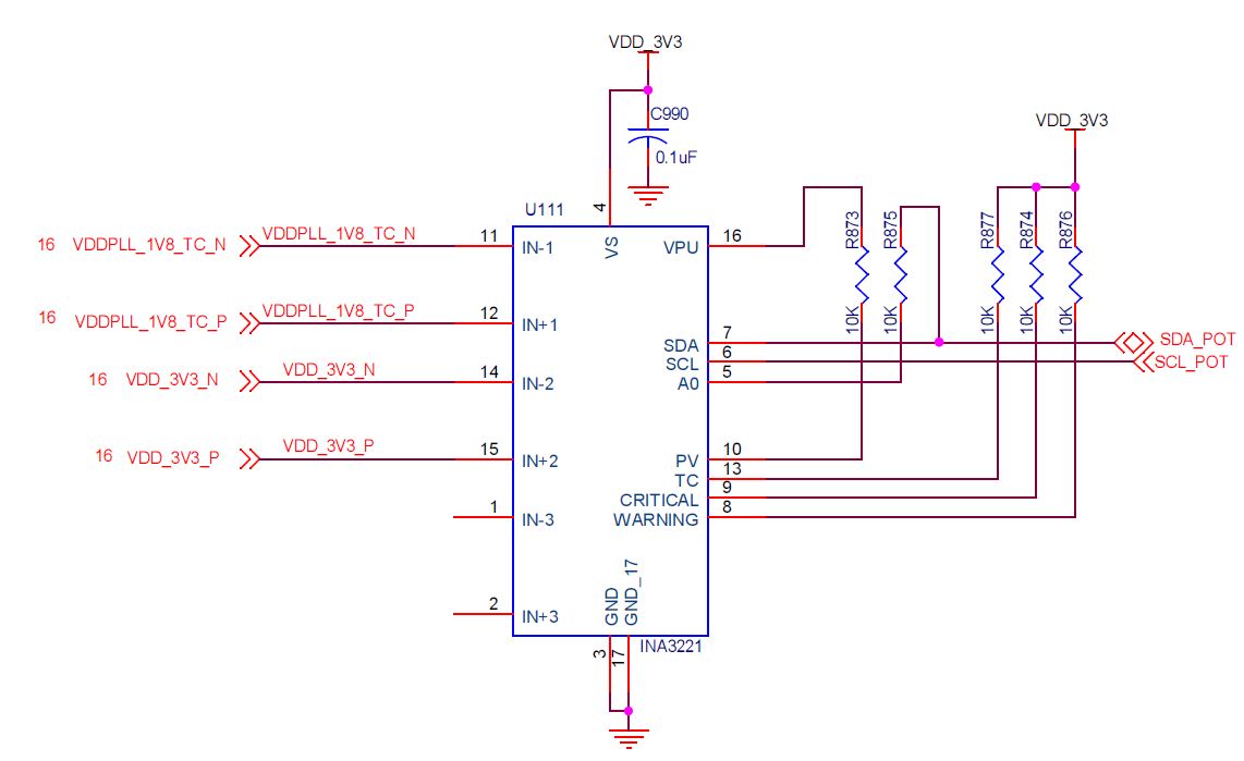
We also observed that when we try to observe the SDA signal on scope and probe (10Mohm 10pf) the resistor R875 (at end towards IC) we are able to read the registers and able to take voltage measurements. Speculating that probe is adding capacitance (10pf) and that capacitance is somehow effecting the bus. But we don't see anything mentioned in device document about capacitance requirement when A0 is connected to SDA.

Note: We are also observing this issue on other platforms which use 4 INA's where the problem is with devices where A0 is connected to SDA/SCL.  

  • Hello Teja,

    Thanks for considering to use Texas Instruments. I need to clarify a few things to determine what might be wrong with your device or setup. You say that the device is unable to communicate. So is the slave INA3221 sending a nack after each transmission from the master? If so, you are saying that the device gives an acknowledge and a proper response when the oscilloscope probe is connected? Is the reading transmitted to the master when the probe is connected correct? By any chance do you have split ground planes? If your slave is at one ground potential and your master is at another ground potential, this could cause issues. In the mean time I will check with my team to see if the capacitance or something else could be contributing to your issue.
  • Hi Patrick,

    We have used active probe (R: 100k  C:700 fF) on channel 1 and passive probe channel 2 (R: 10M C:11pF) and captured some wave forms. It looks like the INA is unable to pull down the SDA line when A0 is connected to SDA. For all the captures we are setting register pointer to 0x0.

    Below capture when CH1 is connected to SDA and CH2 is connected to SCL for failing INA (A0 connected to SDA).

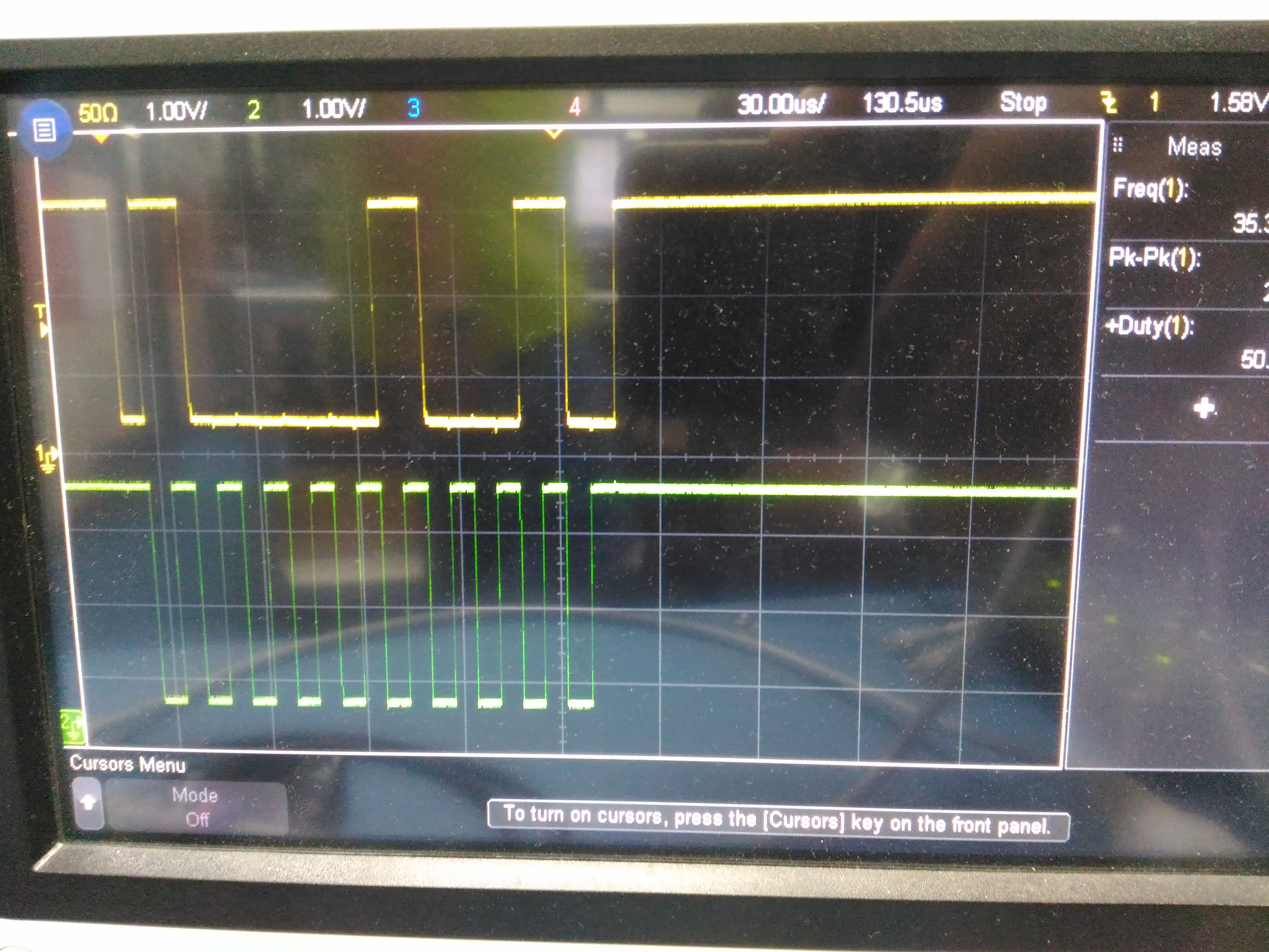
     Below capture when CH1 is connected to SDA and CH2 is connected to SCL for working INA (A0 connected to GND).

    Below capture when CH1 is connected to SCL and CH2 is connected to SDA for failing INA (A0 connected to SDA).

    As you can see when we connect SDA to channel 2 the INA is able to pull down the SDA line and the data is correct.

    We do not have split GND plane on our board, master and slave are on same plane.

    Also we have a TCA9406 voltage translator on the bus which is translating 1.8v to 3.3v before lines go to INAs. This Translator has in-built 10K pull-up on both SDA and SCL lines.

  • Hello Teja,

    I need to run this issue by some our design engineers to determine why this might be happening. However, in the interim, I did look at our EVM schematic/layout files and noticed that we do not use a pull-up resistor between A0 and any of the pins used for setting the address. In fact a jumper short was used. Consequently, I think you may want to replace your 10k between A0 and SDA with a short.
  • Hello Teja,

    Just spoke with one of our design engineers. He echoed that there should not be a 10k between A0 and SDA. He said that by putting the resistor there you are creating an undesirable condition for the internal detection circuit at A0. Once you swap out this 10k with a short, let me know below if you still run into communication issues. Otherwise for now, I think this should resolve your issue.
  • Hi Patrick,

    We have replaced the 10K resistor with short but the issue is still the same. But now the data is not coming correctly even when we connect probe.

  • Hello Teja,

    Sorry to hear that did not work. I will look further into this issue and probe around in the lab to see if I can duplicate your issue. As such it may take a day or so before I have a response for you.
  • Hello Teja,

    So I did some tests in the lab with our EVM and had some difficulties duplicating your results. However, I discussed this with my colleagues and we think that your speculation about capacitance helping may be valid. From looking at the scope shots you provided, we noticed that the part fails to acknowledge when the SDA line drops faster. When talking with one of our design engineers he mentioned that the data hold time specification in the datasheet is likely not correct and should be similar to that of the data hold spec found in our INA226 datasheet (10-900ns). With that in mind the RC constant of your probe (100k with 700fF) is 70ns and within a few RC periods your signal should drop below VIL threshold. So we think more capacitance may satisfy a potentially long data hold time.
  • Hi Patrick,

    If I understand this correctly, you are saying that when A0 is connected to SDA we are getting hold time violation due to added logic in the SDA path. We need to delay the edge of the SDA to increase the hold time and adding the probe is increasing SDA fall time thus delaying the edge and satisfying hold time requirement. Is this correct?
  • Hello Teja,

    Yes it looks as though your master device may not provide sufficient hold time for our INA3221 when A0 is connected to SDA. By adding a pF size cap from the passive probe, it looks as though the falling edge of the SDA is delayed and the INA3221 is able to capture the address value high bits.
  • Hi Patrick,

    I have measured the time between falling edge of SCL and falling edge of SDA, it is 125ns, I have checked with different frequencies. When I put 10k resistor on A0 and probe at the resistor this is forming RC circuit (10k,11pf), now the delay between SDA and SCL negative edges is 235ns and the INA is responding. Can you please measure the delay between SCL and SDA negative edges on your setup? perhaps your setup has more delay and that is why you are unable to replicate this issue. The master we are using is TI MSP430F5500 @ I2C Frequency 71kHz.
  • Hello Teja,

    Our EVM appears to use a clock frequency around 13kHz.  The times between SCL falling edge and SDA falling edge for two of the high address bits in the image below were 26us and 21us.  So that is likely why we never have any issues.

  • Hi Patrick,

    So, I have tried with 10kHz clock also but MSP430F5500 is giving 125ns delay irrespective of clock speed. Do you have any way to increase this delay with MSP430F5500? . Also 125ns is within the spec you mentioned (10-900ns) so why is INA not able to capture the data correctly?. Now I am not sure if this is the problem with master MSP430 which is not satisfying hold time requirements or the slave which is unable to capture the data even when the hold time is within the spec. If this is a problem with MSP430F5500, I will be posting another question relating to this.
  • Hello Teja,

    Besides a capacitor, I do not have a good way to increase the delay.  As for this issue, I did a little more digging and discussed it with another design engineer.  He had a different theory that you might check.  He thinks that your A0 pin may be seeing a lot of noise which could be throwing off the internal detection circuit.  With respect to that, does the communication always fail or does it intermittently work?  One test he suggested for determining whether A0 is noisy is to use your setup that typically fails with A0 connected to SDA and send the address for A0 connected to SCL.  If the device responds in this test, a lot of noise likely is coupling into the A0 pin.  If you can confirm this, then we can look into a solution for reducing that noise.

  • Hi Patrick,

    Do we need to just send the address to the device as if A0 is connected to SCL or do we actually have to connect A0 to SCL instead of SDA?

  • Hello Teja,

    For this test we would like you to keep A0 connected to SDA.  The detection circuit cycles through comparing the voltage potentials, with three potentials checked and the SCL potential treated as the else condition.

  • Hi Patrick,

    The communication always fails when A0 is connected to SDA. I have checked on other boards which have 4 INA's for one of which A0 is connected to SCL on these type of boards the INA whose A0 is connected to SCL is failing intermittently. The INA whose A0 is connected to SDA is always failing on these boards also.

    We are also using 4 INA's on a different board with short I2C lines, on that board all INA's are working. So, this may be a signal quality issue.

  • Hello Teja,

    According to what you just said, the noisy A0 hypothesis could be a closer explanation as to what is happening.  My next step for you would be to depopulate the device connected to SCL and see if the A0=SDA connected device turns on from an A0=SCL address message.  As for the reason the A0=SCL device intermittently fails, it could be an arbitration issue in which both devices think they are A0=SCL.  For your boards with with long I2C lines, do these lines pass over or near any switch-nodes of a switch mode power supply?

  • Hello Teja,

    It's been some time since your last post, so hopefully your issue is resolved. If you need further assistance, please reply to Patrick's latest response so we can continue to help you.

    Best regards,

    Ian Williams
    Applications Manager
    Current & Magnetic Sensing