This thread has been locked.

If you have a related question, please click the "Ask a related question" button in the top right corner. The newly created question will be automatically linked to this question.

OPA2188: Buffering large AC signals and THD

Part Number: OPA2188
Other Parts Discussed in Thread: OPA2196, OPA2189, OPA189

Recently i got a strange distortion out of OPA2188. It distorts even earlier then the data sheet specified slew rate limit of 0.8V/us. And additionally distorts not just as slew limit, but actually decreases output signal level much more.

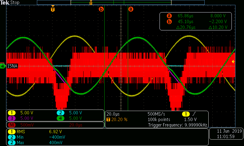
Using a +/-13.5V supply and inputing a 10Vp, 10kHz signal i got following output signal after three OP-Amp stages with OPA2188.

Channel 1: Input Signal, Channel 2: Output Signal after three stages, Channel 4: Output after two stages.

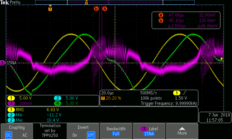
Looking on input of N302.2 shows large ringings during distortion phases:
What is the reason for this and is there a good way to improve/fix it?

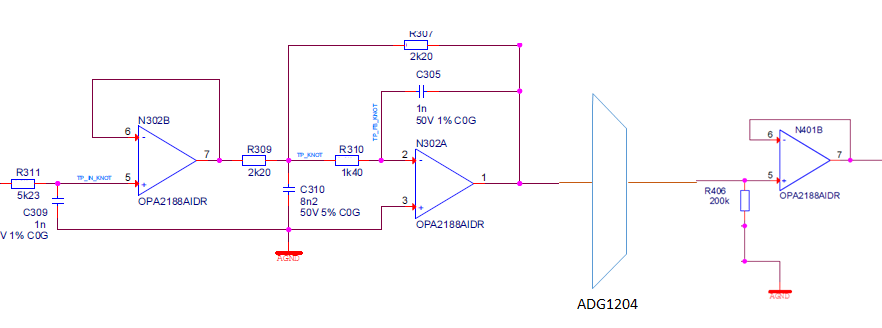
Schematic:
Update: OPA2196 looks promising as drop in signal path alternative ... Let's wait for the samples.

  • Hello Thomas,

    The OPA2188 Op amp stages look okay upon review. Their OPA2188 slew rate should be sufficient for a 10 kHz, 10Vp sine wave.

    It appears that the channel 1 and channel 4 DSO outputs - after two stages look clean, but after the ADG1204 and N401B stage that the output becomes distorted as seen in the DSO channel 2 result. The N401B stage is a simple buffer and I wouldn't expect it to be causing the distortion unless possibly there is something connected to its output that is loading the stage unexpectedly. 

    Are you using the same +/-13.5 V supply for the ADG1204? Its dual-supply datasheet specifications are with +/-15 V supplies, where Vs is +/-10 V. Its maximum Vs might not be a high with +/-13.5 V supplies. If that is the limitation, then changing the Op amp to OPA2196 shouldn't resolve this issue.

    Regards, Thomas

    Precision Amplifiers Applications Engineering

  • Hello Thomas,

    thank you for the good hints, where to look for the reasons. So far I found this effect in output of N302B as well. Just with smaller distortion magnitude.

    Channel 1: Input Signal, Channel 2: Output with MUX off (not important here), Channel 3: N302B.5, Channel 4: N302B.7

    Math = Channel 3- Channel 4

    The input currents raise significantly during distortion, (might not be a bias current, but maybe from input protection circuitry -> a simple input diode model didn't gave me similar enough results)

    I haven't tested for all possible reasons right now, but i'm working on it.

    Best regards,

    Thomas

  • Well that green curve which I believe is the output of the input stage buffer sure looks it is getting slew limited. And yes, Figure 31 in the data sheet shows the negative going slew rate is quite a bit slower than positive. The part specifies a 0.8V/usec typical and 10kHz 10Vp requires .63V/usec - I would be betting this is a lower negative going slew rate causing this. You could certainly test easily with lower amplitudes and see if you "distortion" goes away at say +/-2V swing. 

  • Hi Thomas,

    It looks like Michael is correct regarding the OPA2188 negative slew rate limit being the cause of the distortion. The distortion appears to be worse when the output signal crosses from 0 V and goes negative, where the sine wave dv/dt is maximum. If you can reduce the input frequency as a test and you see the distortion become reduced, then that confirms this is source of the distortion.

    If your application can afford higher operating current the OPA2189, which is also a chopper Op amp, has a much higher slew rate of 20 V/µs. Here's a link to the OPA2189 datasheet:

    http://www.ti.com/lit/ds/symlink/opa2189.pdf

    Regards, Thomas

    Precision Amplifiers Applications Engineering

  • Hello Thomas, 

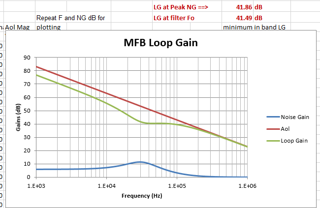
    I had some time and need to navigate my MFB design tool every once in awhile, what you have shown is this design target, 

    your solution is fine, although my tool says it is using to slow an op amp unless a GBP adjust flow is being used - slightly off in response probably - the thing I like to look at is the loop gain profile, Looks ok, a little more noise gain peaking than necessary - 

    If I redesign for the same target shape but less noise gain peaking I can improve the min LG a bit, 

    This helps production spread a bit, 

    here is what the new values look like, and these would change again for a OPA2189 implementation. And yes, the DC gain is slightly over 1.0 - the last step in this flow tests the 8 permutations of standard R values around the exact solution for min nominal error to target Fo and Q - and it lets the DC gain step off one standard value if that is the best Fo and Q fit solution. Normally can make that gain error up somewhere else. 

    And here is the TINA file for the MFB filter, 

    OPA188 MFB filter.TSC

  • Morning Thomas

    I wanted to get the OPA189 into the MFB tool and run it - one issue I was running into (where it was scaling the R values up quite a bit) was to account for how much of the available "linear" output current is being used in the feedback R. The OPA2188 and OPA2189 both have relatively low output current before the required headroom increases rapidly - I usually allow for a 0.5V headroom increase in these kind of parts for an allowed "linear" output current - once you are over 0.5V headroom, you are not really RRO anymore. Anyway, I had the tool setup to only allow 20% of linear in the feedback R, increased that to 40% to get a lower R solution and still leave something to drive a load with. 

    here is the LG plot for the OPA189 solution - it has plenty of GBP margin at 14Mhz.

    OPA189 MFB filter.TSC

  • Hello Michael and Thomas,

    thank you for your vrey good help. Thanks to your hints i could find the cause and fix the issue with the faster op amp. Now no more slewing is occuring. The negative slew rate of OPA2188 really must have been a bit to low for this kind of application. With more then 0.8 V/us all works fine.

    Best Regards,

    Thomas