This thread has been locked.

If you have a related question, please click the "Ask a related question" button in the top right corner. The newly created question will be automatically linked to this question.

TIPD102: Modify design for lower load compliance and higher load current

Part Number: TIPD102
Other Parts Discussed in Thread: TINA-TI

Hello,

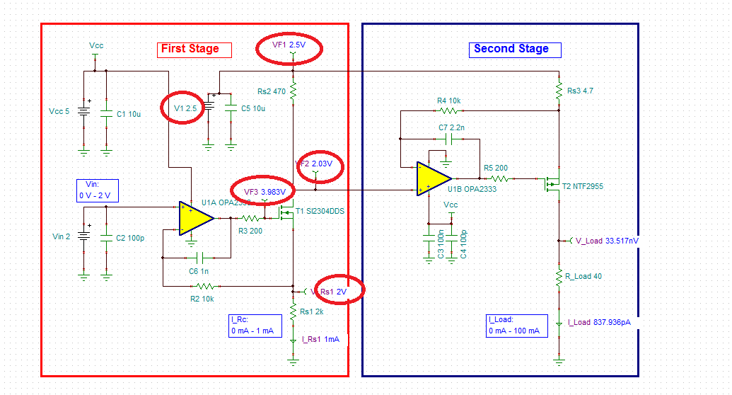
I am developing a custom laser current driver and I saw the application note TIPD102. In my application I would need to operate the laser with a max input current at 300 mA and voltage compliance of 1.5 V. Moreover I would need to set V+ = 2.048 V to match a DAC that would communicate with my PC. 

Looking at the related Tina-TI file, I tried to modify the values to match my requirements, but as soon as I reduce the value of V+ below a certain value (4.5V) the second stage of the system fails to provide voltage and therefore the I_load drops to very small values, due to the lack of voltage at the gate of the mosfet at the systems óutput. It seems to me that the issue might be related with the input of the second amplification stage, where by setting V+ to a low value, the inverting and non-inverting inputs have a values too far apart for the opa to work properly. 

Would someone be able to solve my issue? If I have not been clear I will try to provide more info.

Thank you in advance,

Francesco 

  • Please provide a modified schematic having the issue.

  • Tina Sim FINAL_NTF2955_Compliance - francesco.TSC 

    Hello, 

    thank you for your quick reply.

    I attached the file here. Ideally my schematic is exactly the same as the one found in the application note with the only difference that the voltage that supply the opamps is let at 5V and V+ can be set at a different value, in my case ideally at 2.048V. 

    Many thanks,

    Francesco

  • The problem with your circuit is that you lowered V1 supply to 2V and you attempt to get 2V at V_Rs1 - that is NOT possible since VDS=0 and T1 MOSFET operates in a non-linear fashion (triode region). 

    Thus, in order to fix the problem you have to increase V1 supply to 2.5V or lower Vin to 1.5V - see below.  Increasing V1 to 2.5V fixes the problem and I_Rs1 is at 1mA as expected - see below.

    However, T2 P-channel MOSFET model is not correct so the second stage does NOT work properly. Replacing T2 with pnp transistor fixes the problem and I_Load becomes 100mA as expected - see below.

    e2e.ti.com/.../Tina-Sim-FINAL_5F00_NTF2955_5F00_Compliance-_2D00_-francesco_5F00_edited.TSC

  • Hello,

    thank you very much for your quick reply. Indeed this works well.

    I have a further question. As a second part of your response you said:

    "However, T2 P-channel MOSFET model is not correct so the second stage does NOT work properly. Replacing T2 with pnp transistor fixes the problem and I_Load becomes 100mA as expected - see below."

    Is this a fundamental issue with using the MOSFET or is something to do with the Tina-TI model of the MOSFET? The reason why I ask this is because I have seen different versions of my scheme that were drawn with the MOSFET  also in the second stage (in that case it was a BSO201SPHXUMA1 for which I do not have a Tina-TI model). Indeed if I operate the system with the original V1 = 5V the MOSFET does the job properly, and it starts misbehaving when V1 is reduced.

    If you could clarify this, it would be a great help for me.

    Kind Regards,

    Francesco


  • It is not an issue with Tina-TI since as you can see the circuit works fine with pnp transistor.   The problem is with the p-channel T2 MOSFET model.   Pick the actual FET transistor from any manufacturer and simulate the model that comes with it - things should work just fine.